3D Optical Profiler Market Size, Share, Demand Report By Technology (Confocal Microscopy, Focus Variation, Structured Light Profiling, Others), By Application (Medical Device Surface Analysis, Automotive Component Inspection, Aerospace Component Measurement), By End-Use Industry (Healthcare & Medical Devices, Automotive, Aerospace & Defense, Industrial Manufacturing, Research Institutions), By Region & Segment Forecasts, 2026–2034
USD 3950
Market Overview
The global 3D Optical Profiler Market size was valued at USD 1.48 billion in 2026 and is projected to reach USD 3.29 billion by 2034, expanding at a CAGR of 10.5% during 2026–2034. The market is witnessing consistent growth as industries increasingly adopt high-precision surface metrology solutions for quality control, product development, and manufacturing optimization. 3D optical profilers provide non-contact measurement capabilities that enable accurate characterization of surface roughness, texture, step height, and dimensional features across a wide range of materials and components.
One of the major global factors supporting market expansion is the rapid advancement of precision manufacturing across semiconductor, electronics, automotive, aerospace, and medical device industries. Manufacturers are increasingly focused on achieving tighter tolerances, reducing production defects, and improving product reliability. As a result, demand for advanced inspection technologies capable of delivering high-resolution three-dimensional surface analysis has increased significantly. The transition toward automation and smart manufacturing environments has further accelerated the integration of optical profiling systems into production workflows.
Key Highlights
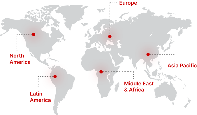
- North America dominated the market with a 35.1% share in 2025.
- while Asia Pacific is expected to grow at the fastest CAGR of 12.4% during 2026–2034.
- By technology, White Light Interferometry accounted for the largest share of 42.8%.
- while Confocal Microscopy Systems are projected to grow at a CAGR of 12.9%.
- By application, Semiconductor Inspection led with a 39.6% share.
- whereas Medical Device Surface Analysis is expected to expand at a CAGR of 12.7%.
- By end-use industry, Electronics and Semiconductor Manufacturing held the largest share of 37.9%.
- while Healthcare and Medical Devices are projected to grow at a CAGR of 12.5%.
- The United States remained the dominant country, with market values of USD 428 million in 2024 and USD 472 million in 2025.
Market Trends
Integration of Artificial Intelligence in Surface Metrology
Artificial intelligence is becoming increasingly important in modern optical profiling systems. Manufacturers are incorporating machine learning algorithms into software platforms to automate defect detection, classify surface irregularities, and improve measurement repeatability. AI-assisted analytics reduce manual inspection requirements and enable real-time decision-making within manufacturing environments. This trend is particularly visible in semiconductor fabrication and electronics production facilities where inspection speed and accuracy are critical. The combination of AI and optical metrology allows organizations to analyze large volumes of measurement data more efficiently, supporting predictive quality control strategies and improving manufacturing productivity while reducing operational costs.
Growing Adoption of Automated Inline Inspection Systems
Industrial manufacturers are increasingly deploying automated inline inspection systems equipped with 3D optical profilers to support continuous quality monitoring. Unlike traditional offline inspection methods, inline solutions provide immediate feedback during production processes, helping manufacturers identify defects before products move to subsequent manufacturing stages. The trend is gaining momentum across automotive, aerospace, semiconductor, and precision engineering sectors where production efficiency and product consistency are major priorities. Advancements in robotics, machine vision, and high-speed imaging technologies are making automated profiling systems more practical for large-scale deployment. Consequently, demand for integrated optical metrology platforms continues to expand across advanced manufacturing environments.
Market Drivers
Expansion of Semiconductor Manufacturing Facilities
The rapid expansion of semiconductor manufacturing facilities worldwide is a major factor driving demand for 3D optical profilers. Semiconductor devices require highly accurate measurement of wafers, microstructures, and nanoscale surface features to ensure product performance and reliability. Optical profilers provide non-contact measurement capabilities that help manufacturers maintain stringent quality requirements throughout fabrication processes. Increasing investments in advanced chip production facilities, growing demand for artificial intelligence hardware, and rising adoption of consumer electronics are generating substantial opportunities for metrology equipment providers. As semiconductor geometries continue to shrink, the need for precise surface characterization solutions is expected to strengthen further.
Rising Demand for Precision Quality Control Across Industries
Manufacturers across various sectors are increasingly emphasizing precision quality control to minimize defects and improve operational efficiency. Industries such as automotive, aerospace, medical devices, and industrial equipment rely on accurate surface measurement to verify product specifications and maintain regulatory compliance. 3D optical profilers offer rapid, non-destructive analysis capabilities that enable comprehensive surface inspection without damaging components. The growing complexity of manufactured products has increased the importance of advanced metrology systems capable of measuring intricate geometries and microscopic features. Consequently, organizations are investing in optical profiling technologies to enhance production quality, reduce waste, and improve overall manufacturing performance.
Market Restraint
High Capital Investment and Technical Complexity
The relatively high acquisition cost of advanced 3D optical profiling systems remains a significant challenge for market expansion. High-resolution instruments equipped with sophisticated optics, imaging components, automation modules, and advanced analytical software often require substantial capital expenditure. Small and medium-sized enterprises may face budget limitations that restrict adoption, particularly in developing economies where manufacturing modernization initiatives are still evolving. Beyond initial purchase costs, organizations must also invest in operator training, system calibration, software updates, and ongoing maintenance activities.
Technical complexity further influences adoption rates. Accurate measurement outcomes depend on proper system configuration, environmental control, and operator expertise. In industries with limited metrology experience, implementation challenges can extend deployment timelines and increase operational costs. For example, precision aerospace component manufacturers often require extensive training programs to ensure accurate interpretation of measurement results. These factors can slow purchasing decisions and encourage some organizations to continue relying on conventional measurement techniques. Although technological advancements are gradually improving system usability, cost and operational complexity continue to represent important barriers affecting broader market penetration.
Market Opportunities
Emerging Demand from Medical Device Manufacturing
Medical device manufacturing presents substantial opportunities for 3D optical profiler providers. The industry increasingly requires highly precise surface characterization for implants, surgical instruments, dental products, and microfluidic devices. Regulatory standards emphasize product quality, safety, and performance, creating strong demand for advanced inspection technologies capable of delivering accurate and repeatable measurements. Optical profilers enable non-contact analysis of delicate components without causing physical damage, making them particularly suitable for medical applications. Growing investments in minimally invasive devices, personalized healthcare solutions, and advanced implant technologies are expected to support increasing adoption of optical metrology systems throughout the forecast period.
Expansion of Electric Vehicle and Advanced Battery Production
The global shift toward electric mobility is creating new opportunities for optical profiling technologies. Electric vehicle manufacturers require precise inspection of battery components, power electronics, sensors, and mechanical assemblies to ensure performance and reliability. Surface quality plays a critical role in battery efficiency, thermal management, and component durability. 3D optical profilers help manufacturers evaluate material characteristics, detect defects, and optimize production processes. Rising investments in battery gigafactories and electric vehicle production facilities across Asia Pacific, Europe, and North America are expected to increase demand for advanced metrology solutions. As competition intensifies within the EV industry, manufacturers are likely to prioritize precision inspection technologies to maintain product quality and production efficiency.
Segmental Analysis
By Technology
White Light Interferometry dominated the technology segment and accounted for approximately 42.8% market share in 2024. The technology remains widely adopted because of its ability to provide highly accurate non-contact surface measurements across a broad range of materials and applications. Manufacturers utilize white light interferometry systems for measuring surface roughness, step height, and microstructural features with exceptional precision. The technology is particularly valuable in semiconductor manufacturing, precision engineering, and research laboratories where accurate three-dimensional surface characterization is essential. Its capability to generate detailed surface maps while maintaining fast inspection speeds has strengthened adoption across industries requiring stringent quality control standards and reliable metrology performance.
Confocal Microscopy Systems represent the fastest-growing technology category and are projected to expand at a CAGR of 12.9% through 2034. Growth is being supported by increasing demand for high-resolution imaging of complex surfaces and transparent materials. Confocal technologies offer advantages in measuring steep slopes, intricate geometries, and delicate components that may be difficult to inspect using conventional methods. The technology is gaining traction in medical device manufacturing, advanced materials research, and microelectronics production. Continuous improvements in imaging performance, automation capabilities, and software analytics are further enhancing adoption. As industries pursue greater measurement flexibility and precision, confocal microscopy solutions are expected to experience significant demand growth.
By Application
Semiconductor Inspection held the largest application share at approximately 39.6% in 2024. Semiconductor manufacturers depend on advanced optical profiling systems to evaluate wafer surfaces, microelectronic structures, and nanoscale features throughout fabrication processes. As device architectures become increasingly complex, accurate surface metrology is essential for maintaining production quality and reducing defect rates. Optical profilers provide non-contact measurement capabilities that support comprehensive inspection without damaging sensitive components. Strong demand for artificial intelligence processors, consumer electronics, and advanced communication technologies continues to drive investment in semiconductor manufacturing facilities, reinforcing the segment's leadership position within the market.
Medical Device Surface Analysis is expected to register the fastest growth rate, expanding at a CAGR of 12.7% during the forecast period. The increasing complexity of implants, surgical instruments, dental devices, and microfluidic systems is creating substantial demand for precise surface characterization technologies. Manufacturers must comply with strict regulatory standards related to product safety and performance, making accurate inspection processes increasingly important. Optical profiling systems allow non-destructive evaluation of critical surfaces while delivering highly repeatable measurement results. Rising healthcare investments, expanding medical technology innovation, and growing adoption of personalized medical devices are expected to contribute significantly to the segment's long-term expansion.
By End-Use Industry
Electronics and Semiconductor Manufacturing accounted for approximately 37.9% of total market revenue in 2024, making it the dominant end-use industry segment. The sector relies extensively on advanced metrology solutions to ensure the quality and performance of electronic components, integrated circuits, sensors, and microelectronic assemblies. Optical profilers provide manufacturers with detailed information regarding surface characteristics and dimensional accuracy, helping reduce defects and improve production yields. The increasing complexity of electronic products, combined with growing global demand for consumer electronics and communication devices, continues to drive investment in precision inspection technologies. This strong demand environment supports the segment's leading market position.
Healthcare and Medical Devices is projected to be the fastest-growing end-use industry, advancing at a CAGR of 12.5% through 2034. Growth is being driven by increasing production of advanced medical technologies, including implants, diagnostic equipment, and minimally invasive surgical instruments. Surface quality plays a critical role in the performance, durability, and biocompatibility of medical products, making accurate inspection essential. Optical profiling technologies enable manufacturers to conduct detailed non-contact measurements while preserving component integrity. Expanding healthcare expenditures, rising demand for precision medical devices, and ongoing innovation in biomedical engineering are expected to strengthen adoption of optical metrology systems across this industry segment.
Regional Analysis
North America
North America accounted for approximately 35.1% of the global 3D Optical Profiler Market in 2025, making it the largest regional market. The region benefits from strong investments in semiconductor manufacturing, aerospace engineering, and advanced industrial automation. Major technology developers and metrology equipment providers maintain extensive operations across the region, contributing to continuous innovation. The market is expected to expand at a CAGR of 9.8% through 2034, supported by increasing adoption of automated inspection systems and demand for precision manufacturing solutions.
The United States remains the dominant country within the region. A key growth factor is the ongoing expansion of domestic semiconductor fabrication facilities supported by public and private investments. These projects are creating significant demand for advanced metrology tools capable of measuring increasingly complex microelectronic structures. Growing research activity in nanotechnology and microelectronics further supports demand for high-resolution optical profiling systems.
North American manufacturers are also investing heavily in Industry 4.0 initiatives, driving integration of optical profilers into connected production environments. Automated inspection workflows are becoming increasingly common in electronics and automotive production facilities. The need for real-time process monitoring continues to strengthen demand for advanced optical metrology technologies.
In addition, aerospace companies throughout the region are adopting optical profiling systems to verify critical component dimensions and surface quality. Increasing production of next-generation aircraft and defense systems requires highly accurate inspection solutions, supporting continued market expansion across industrial sectors.
Europe
Europe represented approximately 27.6% of the global market in 2025 and is expected to register a CAGR of 9.9% during the forecast period. The region benefits from a strong industrial base, advanced manufacturing capabilities, and extensive research activities. Countries across Europe continue to invest in precision engineering and industrial modernization programs, supporting adoption of sophisticated optical measurement technologies.
The Germany market leads the regional landscape due to its strong automotive, industrial machinery, and precision manufacturing sectors. A unique growth factor is the country's emphasis on smart factory implementation and production digitization. Manufacturers increasingly deploy optical profiling systems to improve quality assurance and maintain competitiveness in global markets.
European industries are also adopting optical profilers for renewable energy component manufacturing. Wind turbine components, precision mechanical systems, and advanced electronics require accurate surface characterization, creating sustained demand for metrology equipment. Research institutions throughout the region further contribute to market development through technological innovation.
The presence of advanced automotive manufacturers is another important factor supporting growth. Surface inspection requirements for electric vehicle components, sensors, and battery systems continue to increase. As production standards become more stringent, optical metrology technologies are gaining broader acceptance across industrial applications.
Asia Pacific
Asia Pacific held approximately 24.8% of the global market in 2025 and is projected to record the fastest CAGR of 12.4% through 2034. The region is experiencing substantial industrial growth driven by expanding electronics manufacturing, semiconductor production, and automotive development. Rising investments in high-tech manufacturing facilities are increasing demand for advanced inspection technologies.
China remains the dominant country in the regional market. A major growth factor is the country's extensive investment in semiconductor self-sufficiency initiatives and advanced manufacturing infrastructure. The expansion of domestic electronics production continues to create strong demand for optical profiling systems used in quality assurance and process optimization.
The region also benefits from a large concentration of consumer electronics manufacturers. Smartphones, wearable devices, and semiconductor components require highly accurate surface inspection, supporting widespread deployment of optical metrology equipment. Growing production volumes further strengthen demand for automated inspection solutions.
Countries such as Japan, South Korea, Taiwan, and India are also contributing significantly to market expansion. Investments in precision engineering, advanced materials research, and electric vehicle manufacturing are creating new opportunities for equipment suppliers. The increasing focus on manufacturing quality and operational efficiency is expected to sustain strong growth throughout the forecast period.
Middle East & Africa
The Middle East & Africa accounted for approximately 6.3% of global market revenue in 2025 and is forecast to expand at a CAGR of 8.7% through 2034. Although the regional market remains comparatively smaller, increasing industrial diversification initiatives are creating opportunities for advanced metrology technologies. Governments are encouraging development of manufacturing sectors beyond traditional resource-based industries.
The United Arab Emirates represents the leading market within the region. A unique growth factor is the country's growing investment in aerospace maintenance, precision manufacturing, and advanced technology hubs. These initiatives are increasing demand for optical inspection equipment capable of supporting stringent quality requirements.
Industrial modernization programs across the Gulf region are encouraging adoption of automated manufacturing technologies. Organizations are investing in advanced quality control systems to improve productivity and competitiveness. As industrial capabilities continue to expand, demand for precision measurement tools is expected to increase steadily.
Research institutions and technology development centers are also contributing to market growth. Collaborative projects involving advanced materials, electronics, and engineering applications are creating additional demand for high-resolution surface characterization technologies. These developments are gradually strengthening the regional market position.
Latin America
Latin America captured approximately 6.2% of the global market in 2025 and is expected to grow at a CAGR of 8.9% through 2034. Increasing industrial activity, modernization of manufacturing facilities, and expansion of automotive production are supporting market development. Demand for advanced inspection solutions is rising as manufacturers seek improved product quality and operational efficiency.
Brazil remains the dominant country across the region. A key growth factor is the country's expanding automotive and industrial manufacturing sectors, which increasingly require advanced metrology systems for quality assurance. Investments in production modernization are creating favorable conditions for adoption of optical profiling technologies.
The region is also experiencing growth in electronics assembly and precision component manufacturing. As organizations pursue higher production standards, demand for accurate surface measurement solutions continues to increase. Optical profiling systems provide manufacturers with capabilities needed to support evolving quality requirements.
Government initiatives promoting industrial competitiveness and technological advancement are further supporting market expansion. Although adoption rates vary across countries, ongoing investments in manufacturing infrastructure and quality improvement programs are expected to create steady opportunities for market participants throughout the forecast period.
Competitive Landscape
The 3D Optical Profiler Market is characterized by continuous technological innovation, strategic partnerships, and product development initiatives aimed at improving measurement accuracy and automation capabilities. Market participants are focusing on software integration, artificial intelligence-enabled analytics, and high-speed inspection technologies to strengthen their competitive positions.
Bruker Corporation remains a leading participant due to its extensive portfolio of surface metrology solutions and strong global presence. The company continues to invest in advanced optical measurement platforms designed for semiconductor, industrial, and research applications. Recent developments include enhanced automated analysis capabilities and improved integration with smart manufacturing environments.
Other significant companies include Zygo Corporation, Sensofar Group, KEYENCE Corporation, and Olympus Corporation. These organizations are actively introducing next-generation optical profiling systems featuring higher imaging resolution, faster data acquisition, and advanced software functionality. Competitive strategies also include regional expansion, distribution partnerships, and targeted product launches addressing the needs of semiconductor, electronics, healthcare, and precision manufacturing industries. As demand for advanced metrology solutions increases, competition is expected to remain focused on innovation, operational efficiency, and application-specific performance enhancements.
Key Players
- Bruker Corporation
- Zygo Corporation
- Sensofar Group
- KEYENCE Corporation
- Olympus Corporation
- Nikon Corporation
- Hitachi High-Tech Corporation
- KLA Corporation
- Mitutoyo Corporation
- Alicona Imaging GmbH
- Nanovea Inc.
- Taylor Hobson Ltd.
- Mahr GmbH
- Carl Zeiss AG
- Hexagon AB
Recent Developments
- Bruker Corporation introduced an enhanced automated 3D optical profiling platform featuring advanced AI-assisted defect analysis capabilities for semiconductor manufacturing applications.
- KEYENCE Corporation expanded its optical metrology portfolio with a new high-speed surface inspection system designed for inline industrial quality control environments.
- Zygo Corporation launched an upgraded interferometry-based profiling solution offering improved measurement resolution and faster data processing capabilities for precision engineering applications.
- Sensofar Group introduced advanced software analytics tools that improve automation, reporting efficiency, and integration with smart manufacturing systems.
- KLA Corporation expanded its semiconductor metrology solutions through the development of next-generation surface characterization technologies targeting advanced chip fabrication facilities.
3D Optical Profiler Market Segments
Technology
- White Light Interferometry
- Confocal Microscopy
- Focus Variation
- Structured Light Profiling
- Others
Application
- Semiconductor Inspection
- Medical Device Surface Analysis
- Automotive Component Inspection
- Aerospace Component Measurement
- Materials Research
- Industrial Quality Control
End-Use Industry
- Electronics & Semiconductor Manufacturing
- Healthcare & Medical Devices
- Automotive
- Aerospace & Defense
- Industrial Manufacturing
- Research Institutions
By Region
- North America
- Europe
- APAC
- Middle East and Africa
- LATAM