ABF (Ajinomoto Build-up Film) Substrate Market Size, Share & Trends Analysis Report By Substrate Type (4–8 Layer ABF Substrates, 8–16 Layer ABF Substrates, Above 16 Layer ABF Substrates), By Application (AI GPUs, AI Accelerators, Server CPUs, Networking ICs, PCs & Game Consoles, Other Applications), By End Use (Data Centers & HPC, Consumer Electronics, Automotive, Telecommunications, Other End Uses) and By Region (North America, Europe, APAC, Middle East and Africa, LATAM) Forecasts, 2026–2034
USD 3950
ABF (Ajinomoto Build-up Film) Substrate Market Size
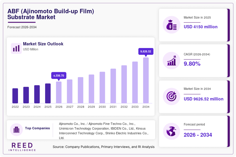
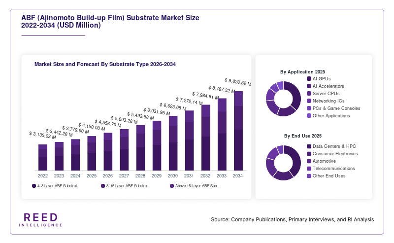
The global ABF (Ajinomoto Build-up Film) Substrate Market size was valued at USD 4,150 million in 2025 and is projected to grow from USD 4,560 million in 2026 to USD 9,690 million by 2034, registering a CAGR of 9.80% during the forecast period from 2026 to 2034.
The ABF substrate market is moving from a PC- and general-server-oriented demand structure toward one increasingly shaped by AI accelerators, high-performance computing, large server CPUs, networking ASICs, and multi-chip packages. ABF is the dielectric build-up material used to create multilayer high-density semiconductor package substrates, and Ajinomoto describes it as a core insulating material for high-performance CPUs and advanced semiconductor packages. The company says ABF has become a de facto standard in this application and is being evolved for servers, data centers, generative AI, GPUs, and next-generation packages.
The demand mechanism is not simply higher semiconductor unit shipments. AI processors increasingly require larger package footprints, more layers, finer wiring, higher I/O density, and stronger control of electrical loss and warpage. Samsung Electro-Mechanics, for example, identifies large-area, high-layer-count substrates and fine circuits as requirements for AI semiconductor packages. TOPPAN likewise markets FC-BGA substrates for AI processors, GPUs, server CPUs, networking devices, and automotive SoCs.
Supply is responding through substantial capacity commitments. IBIDEN approved approximately JPY 500 billion of electronics investment for FY2026–FY2028, primarily targeting high-performance IC substrates for AI and high-performance servers. AT&S is expanding high-end IC-substrate capacity in Malaysia under agreements with AMD and another major technology company. Unimicron has also increased investment in ABF substrates and high-end PCB capacity.
Abf Ajinomoto Build Up Film Substrate Market Drivers
AI accelerators are increasing substrate content per package:
The most important structural change is the increasing amount of substrate engineering required beneath AI processors. Modern AI packages combine high-performance logic with high-bandwidth memory and increasingly complex chiplet architectures. Samsung Electro-Mechanics states that AI semiconductors require large-area, high-layer-count substrates, high circuit density, microvias, and large-scale bump implementation. Ajinomoto has similarly identified HPC, AI applications, multi-chip packages, and 3D-IC as strategic ABF growth areas. Its earlier roadmap showed the server/network share of ABF applications increasing while PC exposure declined. This creates a direct market mechanism: each move toward larger AI packages and higher I/O density requires more sophisticated build-up substrate structures, increasing ABF substrate content and the value of qualified substrate capacity.
High-performance computing is shifting the product mix toward high-layer substrates:
The substrate market is increasingly differentiated by layer count, body size, line/space capability, warpage control, and electrical performance. TOPPAN's current FC-BGA portfolio includes multi-chip, ultra-multilayer, coreless, and 2.3D/2.5D substrates, while supporting applications including server, AI, network, GPU, and automotive processors. Kinsus reports progress in ultra-thin substrates, fine-line circuitry, and large-area, high-layer-count ABF substrates, while concentrating its portfolio on high-end FCBGA and SiP applications. The commercial effect is a shift toward higher-value substrates rather than proportional growth in standard package volumes.
Semiconductor manufacturers are committing capital to advanced packaging capacity:
The substrate industry is responding to customer demand through large, long-duration investments. IBIDEN's JPY 500 billion plan is designed to expand high-performance IC substrate capacity from FY2027 onward. Samsung Electro-Mechanics announced a long-term investment strategy of approximately KRW 15 trillion for package substrates and MLCCs serving AI data-center servers. AT&S has agreed with AMD and another technology company to expand high-end IC substrate production in Kulim, Malaysia, with investment of EUR 1.5–2.0 billion for FY2026/27. These investments increase future supply while simultaneously validating advanced AI substrate demand.
ABF Ajinomoto Build Up Film Substrate Market Restraints
Long qualification cycles and manufacturing complexity limit rapid capacity additions:
ABF substrate capacity cannot be expanded as quickly as conventional PCB capacity because advanced products require fine-line formation, multilayer build-up, laser drilling, plating, inspection, yield optimization, and customer qualification. The substrate must also meet stringent requirements for warpage, thermal performance, signal integrity, and reliability. TOPPAN's technology portfolio illustrates the process complexity, including hyper build-up structures, fine-pitch FC bumps, and line/space down to 10/10 µm. As AI packages become larger and more complex, additional layers increase manufacturing cycles and yield exposure. This can create temporary supply constraints even when manufacturers announce new factories or equipment.
Concentration in the upstream ABF-material supply chain creates dependency:
Ajinomoto remains the dominant supplier of ABF insulation film. The company states that ABF has an overwhelming share of the interlayer-insulation market and supplies the material to semiconductor package-substrate manufacturers. This concentration gives upstream material availability strategic importance for the entire substrate ecosystem. At the same time, substrate makers remain geographically concentrated in East Asia, particularly Japan, Taiwan, South Korea, and other Asian production hubs. A disruption at the material, equipment, substrate, or advanced-packaging level can therefore affect multiple downstream semiconductor programs simultaneously.
ABF Ajinomoto Build Up Film Substrate Market Opportunities
Expansion of AI server and networking substrate platforms:
AI infrastructure is broadening beyond GPUs to custom accelerators, CPUs, networking ASICs, switches, and other data-center processors. Nan Ya PCB is developing ABF substrates for AI PC processors, AI GPUs, AI ASICs, high-speed switches, Wi-Fi 7 chips, retimers, and high-end transceiver modules. TOPPAN similarly serves AI processors, GPUs, network devices, and server CPUs. This expands the addressable substrate base beyond a small number of GPU programs. As hyperscale data centers deploy multiple processor and networking architectures, substrate suppliers can capture additional demand through qualification across CPUs, accelerators, ASICs, and connectivity silicon.
Next-generation package architectures and materials:
The transition toward chiplets, 2.5D/3D packaging, optical-electrical co-packaging, and larger package bodies creates opportunities for new ABF generations. Ajinomoto's 2026 strategy specifically calls for evolving ABF for advanced semiconductor packages and devices and developing functional materials for photonic-electronic co-packages. Samsung Electro-Mechanics is simultaneously developing 2.5D, 2.1D, and glass-substrate technologies to address increasingly large and integrated AI packages. This creates opportunities for suppliers that can solve fine-line routing, low-loss transmission, dimensional stability, thermal management, and warpage challenges as conventional organic substrates approach their technical limits.
Segmental Analysis
By Substrate Type
8–16 Layer ABF Substrates represent approximately 48% of the global market in 2025, reflecting their broad use across high-performance computing, server processors, networking chips, and other advanced FC-BGA applications. The shift toward greater I/O density is increasing the number of electrical-routing layers required between advanced processors and system boards. Ajinomoto's own ABF development strategy emphasizes increasing package complexity and the growing volume of ABF required per IC as semiconductor packages become larger and more complex.
Above 16 Layer ABF Substrates are the fastest-growing substrate category, with an estimated 12.7% CAGR through 2034. The segment benefits from AI accelerators and multi-chip packages that require more signal routing and power distribution. Samsung Electro-Mechanics highlights the need for high-layer-count structures for AI semiconductors, while Kinsus is specifically developing large-area, high-layer-count ABF substrates.
By Application
AI GPUs account for approximately 31% of the market in 2025, as high-end GPU packages require large substrates capable of routing high numbers of signals between logic dies, HBM, and the system board. Samsung Electro-Mechanics specifically identifies AI accelerators and GPUs as applications requiring large-area and high-density package substrates.
AI Accelerators are the fastest-growing application, registering approximately 13.6% CAGR. The category includes custom accelerators and other purpose-built AI processors deployed in hyperscale and enterprise data centers. Ajinomoto identifies generative AI, GPUs, HPC, and next-generation multi-chip packages as important areas for continued ABF development.
By End Use
Data Centers & HPC represent approximately 54% of the global market in 2025, reflecting the increasing concentration of advanced processors in AI infrastructure. IBIDEN explicitly identifies AI servers and high-performance servers as the target for its new high-performance IC substrate capacity.
Telecommunications is the fastest-growing end-use category at approximately 11.8% CAGR, supported by high-speed networking ASICs, switches, optical communications, and data-center connectivity. Nan Ya PCB is developing ABF substrates for high-speed switches, retimers, and high-end transceiver modules, demonstrating how networking hardware is becoming a larger part of the advanced-substrate opportunity.
Regional Analysis
North America ABF Ajinomoto Build Up Film Substrate Market
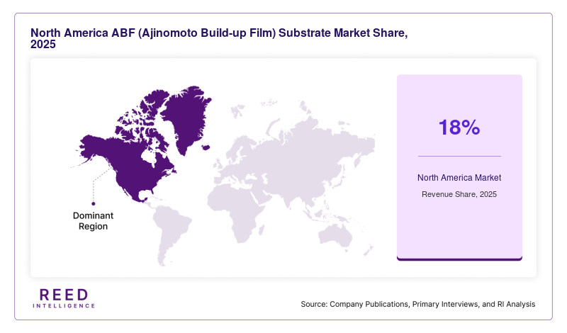
North America represents approximately 18% of the global ABF substrate market in 2025 and is growing at around 9.4% CAGR. The region's importance comes primarily from semiconductor designers, hyperscale data centers, AI accelerator developers, and server manufacturers rather than from its share of global substrate manufacturing. AI infrastructure investment increases demand for GPU, CPU, accelerator, and networking packages that require advanced ABF substrates.
The region's purchasing influence is particularly important because qualification decisions by major processor and cloud-computing companies determine which substrate manufacturers receive production programs. This creates a customer-driven market mechanism in which North American AI hardware investment translates into manufacturing demand primarily in Asian substrate facilities.
The principal limitation is manufacturing concentration outside the region. Much of the advanced ABF substrate supply chain remains based in Japan, Taiwan, South Korea, and other Asian locations. This makes North American semiconductor growth dependent on international substrate capacity and customer-qualified production.
Europe ABF Ajinomoto Build Up Film Substrate Market
Europe accounts for approximately 12% of the global market and is expanding at around 8.8% CAGR. Demand comes from automotive semiconductors, industrial computing, telecommunications, high-performance processors, and European investment in semiconductor manufacturing. TOPPAN's FC-BGA portfolio demonstrates that automotive SoCs and high-end processors are important applications alongside AI and server products.
Automotive is particularly relevant because advanced driver-assistance systems and autonomous-driving architectures require increasingly sophisticated processors. These chips need package substrates capable of handling high I/O density while maintaining reliability across temperature and environmental conditions.
Europe's substrate ecosystem is also strengthening through AT&S. Its Kulim investment is directly linked to high-end IC substrates for AI and HPC, demonstrating how European-headquartered companies are expanding manufacturing capacity in Asia to serve global semiconductor customers.
APAC ABF Ajinomoto Build Up Film Substrate Market
APAC holds approximately 61% of the global ABF substrate market in 2025 and is the fastest-growing region, with a CAGR of approximately 11.1%. The region combines the largest concentration of advanced package-substrate manufacturers with Taiwan's semiconductor ecosystem, Japan's materials and substrate expertise, South Korea's electronics manufacturing base, and expanding Southeast Asian production.
Taiwan remains central through companies such as Unimicron, Kinsus, and Nan Ya PCB. Unimicron increased its 2026 capital expenditure to approximately NT$34 billion, with ABF substrates and high-end PCB production among the major investment areas. The company also reported that AI-related applications represented approximately 40% of ABF-substrate revenue in the prior year and were expected to reach 60% in 2026.
Japan remains critical through Ajinomoto, IBIDEN, and Shinko Electric. IBIDEN's JPY 500 billion FY2026–FY2028 investment plan is explicitly aimed at AI-server and high-performance-server substrates. South Korea is expanding through Samsung Electro-Mechanics, which has announced a long-term package-substrate investment program for AI data-center servers.
Southeast Asia is becoming more important as manufacturers diversify production. AT&S is expanding its Kulim facility in Malaysia, while LG Innotek has announced plans for a new semiconductor-substrate plant in Vietnam. The region therefore combines demand concentration, technology expertise, and manufacturing expansion, supporting its leading position.
Middle East and Africa ABF Ajinomoto Build Up Film Substrate Market
Middle East and Africa accounts for approximately 4% of the global market and is growing at around 10.2% CAGR. The region's demand is primarily indirect, arising from data-center development, telecommunications infrastructure, cloud services, and digitalization rather than a large local ABF-substrate manufacturing base.
Data-center and telecommunications investment creates demand for servers, networking equipment, switches, and accelerators containing advanced package substrates. As regional cloud infrastructure expands, ABF demand can increase through imported servers and networking hardware.
The primary constraint is the limited local substrate manufacturing ecosystem. Consequently, the region remains dependent on global semiconductor and electronics supply chains, while local demand is more closely linked to data-center equipment imports and telecommunications infrastructure spending.
LATAM ABF Ajinomoto Build Up Film Substrate Market
LATAM represents approximately 5% of the global market and is growing at around 9.9% CAGR. Demand is associated with telecommunications, data centers, consumer electronics, automotive electronics, and broader digital infrastructure. Brazil and Mexico provide the largest potential demand centers because of their electronics manufacturing and technology markets.
The regional market remains largely downstream because advanced ABF substrate manufacturing is concentrated in Asia. Growth therefore depends on imports of processors, servers, networking equipment, and electronic systems incorporating advanced substrates.
Over the forecast period, greater data-center investment and AI adoption can increase regional consumption of advanced computing hardware. However, currency volatility, import dependence, and comparatively limited advanced-packaging infrastructure remain constraints on localized market development.
Competitive Landscape
The ABF substrate industry has a concentrated manufacturing structure because advanced FC-BGA production requires substantial capital, long customer qualification cycles, high yields, and sophisticated fine-line and multilayer capabilities. Unimicron, IBIDEN, Kinsus, Shinko Electric, Samsung Electro-Mechanics, Nan Ya PCB, AT&S, and TOPPAN form an important competitive group, although their exposure differs by customer, package type, geography, and technology level. Current industry activity shows that competition is shifting from standard FC-BGA volumes toward large-body, high-layer-count substrates for AI and HPC.
IBIDEN is strengthening its position through approximately JPY 500 billion of FY2026–FY2028 investment, including JPY 220 billion for the first phase of capacity expansion at Gama and other facilities. Production is scheduled to ramp sequentially from FY2027. Unimicron is expanding ABF capacity and high-end PCB production while increasing its exposure to AI applications. Kinsus is concentrating on high-end FCBGA and SiP products and expanding capacity after securing customer recognition for new products.
Samsung Electro-Mechanics is expanding its advanced package-substrate portfolio around AI accelerators, servers, autonomous driving, and data centers while also developing 2.5D, 2.1D, and glass substrates. AT&S is increasing high-end capacity in Malaysia through customer-linked investments with AMD and another major technology company. TOPPAN differentiates through ultra-multilayer, coreless, multi-chip, and 2.3D/2.5D FC-BGA technologies.
Key Market Players
- Ajinomoto Co., Inc. / Ajinomoto Fine-Techno Co., Inc.
- Unimicron Technology Corporation
- IBIDEN Co., Ltd.
- Kinsus Interconnect Technology Corp.
- Shinko Electric Industries Co., Ltd.
- Samsung Electro-Mechanics Co., Ltd.
- Nan Ya PCB Corporation
- AT&S
- TOPPAN Holdings Inc.
- LG Innotek
- Daeduck Electronics
- Kyocera Corporation
- Meiko Electronics
- Zhen Ding Technology
- Compeq Manufacturing
Recent Market Developments
- June 2026 – AT&S reached agreements with AMD and another major technology company to expand high-end IC-substrate capacity in Kulim, Malaysia, committing approximately EUR 1.5–2.0 billion for FY2026/27 capacity expansion.
- June 2026 – Unimicron raised 2026 capital expenditure to approximately NT$34 billion, targeting ABF substrates, high-end PCB production, and additional manufacturing capacity. AI-related applications were expected to account for approximately 60% of ABF-substrate revenue in 2026.
ABF (Ajinomoto Build-up Film) Substrate Market Segments
By Substrate Type
- 4–8 Layer ABF Substrates
- 8–16 Layer ABF Substrates
- Above 16 Layer ABF Substrates
By Application
- AI GPUs
- AI Accelerators
- Server CPUs
- Networking ICs
- PCs & Game Consoles
- Other Applications
By End Use
- Data Centers & HPC
- Consumer Electronics
- Automotive
- Telecommunications
- Other End Uses
By Region
- North America
- Europe
- APAC
- Middle East and Africa
- LATAM