Additive Manufacturing In Semiconductor Industry Market Size, Share, Demand Report By Technology (Metal Additive Manufacturing, Polymer Printing, Stereolithography, Micro-scale Inkjet Printing), By Application (Rapid Prototyping & Tooling, Advanced Packaging Components, Thermal Management Parts, Spare Parts Production), By End Use (Integrated Device Manufacturers, Foundries, OSAT Providers, Equipment OEMs), By Region & Segment Forecasts, 2026–2034
USD 3950
Market Overview
The Additive Manufacturing In Semiconductor Industry Market size was valued at USD 1.18 billion in 2026 and is projected to reach USD 2.86 billion by 2034, expanding at a CAGR of 11.7% during 2026–2034. The market is gaining momentum as semiconductor manufacturers seek faster prototyping, lower material waste, and more flexible production methods for advanced packaging, tooling, wafer handling systems, microfluidic components, and thermal management structures. Additive manufacturing technologies such as metal powder bed fusion, stereolithography, direct ink writing, and micro-scale printing are increasingly integrated into chip fabrication ecosystems where precision and design complexity are critical.
A key global factor supporting market expansion is the rapid rise in demand for high-performance chips used in artificial intelligence servers, automotive electronics, industrial automation, and next-generation communication devices. These applications require faster product cycles and customized component architectures. Additive manufacturing allows semiconductor companies to shorten engineering timelines, optimize cooling channels, reduce tooling lead times, and create lightweight precision parts that are difficult to achieve through subtractive methods. As fabs modernize and governments invest in domestic semiconductor capacity, the need for agile manufacturing tools continues to rise.
Key Highlights
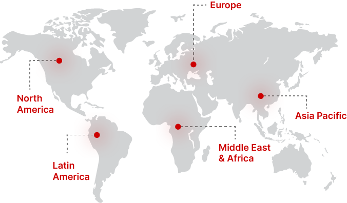
- North America dominated the market with a 36.4% share in 2025.
- Asia Pacific is expected to grow at the fastest CAGR of 13.1% during 2026–2034.
- By technology, metal additive manufacturing accounted for the largest share of 39.2%.
- while micro-scale inkjet printing is projected to grow at a 14.3% CAGR.
- By application, rapid prototyping and tooling led with a 42.6% share, whereas advanced packaging components are expected to expand at a 13.8% CAGR.
- The United States remained the dominant country, with market values of USD 365 million in 2024 and USD 412 million in 2025.
Market Trends
Growing Use of 3D Printing for Semiconductor Tooling
Semiconductor plants are increasingly using additive manufacturing for customized tooling such as wafer carriers, robotic end effectors, vacuum fixtures, alignment jigs, and inspection mounts. These components often require short production runs, high dimensional precision, and resistance to chemicals or heat. Conventional machining can be expensive and slow for such low-volume parts. Additive manufacturing reduces turnaround time from weeks to days, enabling fabs to maintain uptime and quickly modify tools for new process nodes. This trend is especially visible in mature fabs upgrading legacy lines where custom retrofitting is common.
Expansion of Printed Thermal Management Solutions
Heat dissipation is becoming a central challenge in advanced semiconductor packaging. As chip densities rise, manufacturers are adopting additive manufacturing to create complex heat sinks, lattice structures, vapor chamber housings, and optimized cooling geometries. These designs improve airflow and thermal transfer while lowering weight. Additive methods support rapid iteration and topology optimization that conventional fabrication struggles to achieve. Demand is increasing from AI accelerators, power semiconductors, and automotive control modules where temperature control directly affects performance and reliability. This trend is expected to create strong long-term demand for metal printing systems.
Market Drivers
Need for Faster Product Development Cycles
The semiconductor industry operates on aggressive innovation timelines. New chip architectures, packaging methods, and process technologies require continuous prototyping and validation. Additive manufacturing helps engineering teams produce test fixtures, housing components, fluid channels, and package models without waiting for molds or complex machining schedules. This speed advantage lowers time-to-market and supports iterative design workflows. Companies launching chips for AI, consumer electronics, and automotive systems increasingly rely on rapid development tools, making additive manufacturing a practical investment across research centers and production facilities.
Rising Investments in Regional Semiconductor Manufacturing
Governments across North America, Europe, and Asia are funding domestic semiconductor capacity to strengthen supply chains. New fabs and packaging plants require efficient methods for setup, maintenance, and process customization. Additive manufacturing is being adopted during plant construction and ramp-up phases because it can produce spare parts, custom fixtures, cleanroom-compatible accessories, and engineering prototypes locally. This reduces dependence on imported specialty parts and lowers downtime risk. As new fabrication sites scale operations, additive systems are becoming part of broader smart manufacturing strategies.
Market Restraint
Qualification and Reliability Challenges for Production Use
Despite strong growth potential, the Additive Manufacturing In Semiconductor Industry Market faces restraints linked to qualification standards and long-term reliability concerns. Semiconductor manufacturing environments demand extremely tight tolerances, contamination control, thermal stability, and repeatability. Many printed components must undergo extensive testing before use near wafers or cleanroom processes. Material porosity, dimensional drift, surface roughness, and batch consistency can slow adoption for mission-critical applications. For example, a printed wafer handling tool may require repeated validation before approval, delaying deployment. Smaller fabs may hesitate to invest in systems if validation costs exceed short-term productivity gains. These issues are more significant for end-use production parts than for prototyping applications, causing adoption to progress in stages rather than through immediate large-scale replacement of conventional methods.
Market Opportunities
Growth of Advanced Packaging Ecosystems
The rise of chiplets, heterogeneous integration, and 2.5D/3D packaging creates a major opportunity for additive manufacturing suppliers. Packaging lines need custom molds, precision alignment tools, thermal structures, encapsulation fixtures, and rapid prototype carriers. Additive systems can produce these parts faster than conventional methods while supporting frequent design revisions. As semiconductor companies move beyond monolithic chip scaling, packaging innovation becomes central to performance gains. This shift is expected to expand demand for high-resolution printers, engineering materials, and digital manufacturing software tailored to assembly environments.
Adoption by Equipment OEMs and Service Providers
Semiconductor equipment makers and contract engineering firms are emerging as valuable customers for additive manufacturing technologies. OEMs can use printing for spare parts, fluid manifolds, vacuum components, robotics brackets, and demonstration units. Service providers can offer on-demand printed components to fabs that prefer outsourced production. This model reduces capital burden for smaller chipmakers while creating recurring revenue streams for specialized print bureaus. As supply chains seek resilience and local sourcing, outsourced additive manufacturing services are likely to gain traction across multiple semiconductor clusters.
Segmental Analysis
By Technology
Metal additive manufacturing was the dominant technology segment, accounting for 39.2% share in 2024. It is widely used for heat sinks, vacuum manifolds, structural brackets, tooling inserts, and fluid management parts where strength and thermal conductivity are essential. Semiconductor facilities value metal printing for producing complex internal channels and lightweight geometries that improve system efficiency. Stainless steel, aluminum, titanium, and copper-alloy materials are commonly selected depending on thermal and chemical exposure requirements. The segment also benefits from increasing adoption in advanced packaging equipment and inspection hardware where durability is critical.
Micro-scale inkjet printing is expected to be the fastest-growing technology, advancing at a 14.3% CAGR through 2034. This method supports precise deposition of conductive inks, dielectric materials, and fine-feature structures on substrates used in sensors, packaging, and electronics integration. Growth is driven by demand for miniaturized components and flexible production methods. As printed electronics converge with semiconductor assembly, micro-scale printing enables lower material waste and digitally controlled manufacturing. Research institutions and pilot lines are accelerating commercialization, especially for specialized low-volume chip packaging formats.
By Application
Rapid prototyping and tooling held the largest application share of 42.6% in 2024. Semiconductor companies rely on fast production of fixtures, wafer holders, robotic grippers, calibration tools, and process testing assemblies. The ability to redesign and reproduce parts quickly improves fab uptime and shortens engineering cycles. Conventional machining remains important, but additive manufacturing offers clear benefits for low-volume or highly customized tools. Demand is especially strong in facilities operating multiple product generations simultaneously, where equipment adaptation is frequent and standard components may not fit.
Advanced packaging components are projected to grow at the fastest 13.8% CAGR during the forecast period. This includes thermal plates, custom alignment frames, package prototypes, encapsulation molds, and interconnect support structures. Chiplet architectures and heterogeneous integration require frequent design changes and complex geometries that benefit from additive processes. As packaging becomes a larger source of semiconductor performance gains, spending is shifting toward flexible manufacturing tools. Suppliers that deliver high-resolution printing and certified materials are expected to capture expanding opportunities in this segment.
By End Use
Integrated device manufacturers were the dominant end-use segment, representing 46.8% share in 2024. Large chipmakers operate extensive fabrication and packaging networks, making them strong adopters of additive manufacturing for internal tooling, spare parts, and R&D programs. Their scale supports investment in industrial printers, digital workflows, and material qualification programs. These companies also prioritize supply resilience, encouraging in-house production of critical low-volume components. The segment benefits from long-term modernization initiatives across mature and advanced fabs.
OSAT providers are expected to be the fastest-growing end-use segment with a 12.9% CAGR through 2034. Outsourced assembly and testing firms face rising complexity from advanced packaging formats and customer-specific requirements. Additive manufacturing helps them create quick-turn package prototypes, alignment fixtures, and thermal solutions without delaying production schedules. Growth is strongest in Asia Pacific, where large packaging ecosystems continue to expand. As fabless semiconductor models grow, OSAT demand for agile manufacturing tools is likely to rise further.
Regional Analysis
North America
North America held 36.4% of the global market in 2025 and is projected to expand at a 10.9% CAGR through 2034. The region benefits from advanced semiconductor design ecosystems, strong R&D budgets, and high adoption of industrial automation. Demand is concentrated in prototype tooling, packaging innovation, and precision metal printing for thermal management systems.
The United States leads regional revenue generation due to its concentration of fabless chip designers, equipment suppliers, and newly funded manufacturing projects. A unique growth factor is the integration of additive manufacturing into defense and aerospace semiconductor supply programs that require secure, localized production and rapid customization of specialty components.
Europe
Europe accounted for 23.1% market share in 2025 and is forecast to grow at a 10.6% CAGR. Regional growth is supported by automotive semiconductor demand, industrial electronics production, and increasing investment in power semiconductor capacity. Additive manufacturing is widely used for tooling, sensor housings, and cooling components.
Germany is the dominant country within Europe because of its strong engineering base and semiconductor equipment expertise. A unique growth factor is the rapid deployment of printed precision parts for electric vehicle power electronics manufacturing lines, where flexibility and shorter tooling cycles improve production efficiency.
Asia Pacific
Asia Pacific represented 28.7% share in 2025 and is expected to register the fastest 13.1% CAGR through 2034. The region hosts large wafer fabrication clusters, OSAT providers, and electronics exporters. Strong demand comes from scalable prototyping, spare parts localization, and advanced packaging components.
China remains the largest country market, supported by ongoing semiconductor self-sufficiency programs and heavy capital spending on fabrication capacity. A unique growth factor is the fast adoption of additive systems by domestic equipment manufacturers seeking to reduce reliance on imported machined components.
Middle East & Africa
Middle East & Africa captured 6.2% share in 2025 and is projected to grow at a 9.8% CAGR. The market remains smaller but is expanding through electronics assembly investments, industrial diversification, and technology park development. Additive manufacturing demand is centered on maintenance tools and prototype engineering.
Israel leads the region due to its semiconductor design expertise and advanced electronics ecosystem. A unique growth factor is the presence of specialized R&D programs focused on microelectronics innovation, which increases demand for fast-turn custom components and lab-scale fabrication accessories.
Latin America
Latin America held 5.6% share in 2025 and is anticipated to grow at a 9.5% CAGR through 2034. Growth is linked to electronics assembly, industrial automation, and gradual expansion of regional supply chains. Additive manufacturing is used mainly for jigs, fixtures, and replacement parts.
Brazil dominates the regional market because of its broad manufacturing base and growing electronics sector. A unique growth factor is the increasing use of localized printed tooling by contract manufacturers seeking to reduce import delays and lower maintenance downtime.
Competitive Landscape
The market is moderately consolidated, with global industrial printing firms, materials developers, and semiconductor equipment specialists competing through partnerships and application development. 3D Systems Corporation remains a leading participant due to its precision printing portfolio and strong presence in electronics prototyping. A recent development in the industry includes expanded collaborations between printer manufacturers and semiconductor fabs to certify cleanroom-compatible materials.
Other notable companies include Stratasys Ltd., EOS GmbH, Nano Dimension Ltd., and GE Additive. These firms are investing in micro-scale resolution, conductive materials, and software integration for factory workflows. Competition increasingly centers on print accuracy, repeatability, certified materials, and after-sales engineering support. Companies able to offer turnkey solutions for semiconductor packaging and tooling are expected to gain market share.
Key Players List
- 3D Systems Corporation
- Stratasys Ltd.
- EOS GmbH
- Nano Dimension Ltd.
- GE Additive
- Desktop Metal Inc.
- SLM Solutions Group
- Renishaw plc
- HP Inc.
- Trumpf Group
- Materialise NV
- Markforged Holding Corp.
- Formlabs Inc.
- ExOne Company
- Voxeljet AG
Recent Developments
- A leading industrial printer vendor launched a copper-compatible additive platform for thermal semiconductor applications in 2025.
- Several Asian OSAT companies expanded pilot programs using printed package tooling and alignment fixtures in 2025.
- A U.S.-based semiconductor fab adopted on-site additive manufacturing cells for spare parts and maintenance tools in 2026.
Additive Manufacturing In Semiconductor Industry Market Segments
Technology
- Metal Additive Manufacturing
- Polymer Printing
- Stereolithography
- Micro-scale Inkjet Printing
Application
- Rapid Prototyping & Tooling
- Advanced Packaging Components
- Thermal Management Parts
- Spare Parts Production
End Use
- Integrated Device Manufacturers
- Foundries
- OSAT Providers
- Equipment OEMs
By Region
- North America
- Europe
- APAC
- Middle East and Africa
- LATAM