GaN Substrate Wafer Market Size, Share & Demand Report By Type (Bulk GaN Wafer, GaN-on-Silicon Wafer, GaN-on-SiC Wafer), By Application (Power Electronics, RF Devices, Optoelectronics), By End-Use (Telecommunications, Automotive, Industrial, Consumer Electronics, Aerospace & Defense), By Region & Segment Forecasts, 2026–2034
USD 3950
Market Overview
The GaN Substrate Wafer Market size was valued at USD 1.12 billion in 2026 and is projected to reach USD 3.08 billion by 2034, expanding at a CAGR of 13.4% during the forecast period (2026–2034). Gallium nitride (GaN) substrate wafers are gaining traction due to their superior electrical properties, including high electron mobility, thermal stability, and efficiency in high-frequency and high-power applications. These advantages make GaN wafers a preferred choice in next-generation electronics, including power devices, RF components, and optoelectronics.
One major global factor supporting market growth is the rapid expansion of 5G infrastructure and high-frequency communication technologies. The increasing deployment of 5G base stations and satellite communication systems has intensified the demand for GaN-based devices, as they provide improved performance and energy efficiency compared to traditional silicon-based alternatives. Additionally, the ongoing electrification of transportation and the rising adoption of electric vehicles have further accelerated demand for GaN substrate wafers in power electronics.
Key Highlights
- North America dominated the market with a 35.6% share in 2025.
- Asia Pacific is expected to grow at the fastest CAGR of 14.2% during 2026–2034.
- By type, bulk GaN wafers accounted for the largest share of 42.8%.
- while GaN-on-SiC wafers are projected to grow at a CAGR of 15.1%.
- By application, power electronics led with a 39.5% share, whereas RF devices are expected to expand at a CAGR of 14.6%.
- The United States remained the dominant country, with market values of USD 420 million in 2024 and USD 468 million in 2025.
Market Trends
The GaN Substrate Wafer Market is witnessing a growing trend toward the adoption of GaN-on-SiC and GaN-on-Silicon technologies for high-performance applications. Manufacturers are increasingly focusing on hybrid wafer technologies that combine the advantages of different substrates to optimize cost and performance. GaN-on-SiC wafers are particularly gaining momentum in RF and aerospace applications due to their superior thermal conductivity and power density. At the same time, GaN-on-Silicon is being explored for cost-sensitive applications such as consumer electronics and automotive systems. This trend is encouraging innovation in wafer fabrication techniques and driving competition among suppliers to offer optimized solutions.
Another significant trend is the integration of GaN substrate wafers in electric mobility and renewable energy systems. As electric vehicles and solar inverters require efficient power conversion, GaN-based devices are becoming increasingly essential. Automotive OEMs are incorporating GaN wafers in onboard chargers and DC-DC converters to enhance energy efficiency and reduce system size. Similarly, renewable energy systems are leveraging GaN technology for efficient power management. This trend is expected to accelerate as governments promote sustainability initiatives and energy-efficient technologies across industries.
Market Drivers
The increasing demand for high-frequency and high-power electronic devices is a key driver of the GaN Substrate Wafer Market. Industries such as telecommunications, defense, and aerospace require components that can operate efficiently at high frequencies and temperatures. GaN wafers offer superior performance compared to traditional silicon and gallium arsenide substrates, making them ideal for these applications. The growing deployment of 5G networks and radar systems has significantly boosted the demand for GaN-based RF devices. As communication technologies continue to evolve, the need for advanced substrates capable of supporting higher bandwidth and power levels is expected to drive market growth further.
Another major driver is the rising adoption of GaN technology in electric vehicles and power electronics. GaN substrate wafers enable the development of compact, efficient, and lightweight power devices, which are essential for modern EV systems. Automakers are increasingly using GaN-based components to improve battery efficiency and reduce energy losses. Additionally, industrial applications such as data centers and renewable energy systems are adopting GaN technology to enhance energy efficiency. The growing focus on reducing carbon emissions and improving energy utilization is expected to sustain demand for GaN substrate wafers over the forecast period.
Market Restraint
The high cost of GaN substrate wafer production remains a significant restraint for market growth. Manufacturing GaN wafers involves complex processes such as epitaxial growth and defect reduction, which require advanced equipment and expertise. These factors contribute to higher production costs compared to traditional silicon wafers. As a result, small and medium-sized enterprises may find it challenging to adopt GaN technology due to budget constraints. Additionally, the limited availability of high-quality bulk GaN substrates further increases costs and affects supply consistency.
This cost barrier has a direct impact on the adoption rate across price-sensitive applications, particularly in consumer electronics. While GaN offers superior performance, manufacturers often weigh cost considerations when selecting materials. For instance, in applications where performance requirements are moderate, silicon-based alternatives may still be preferred due to their lower cost. Although ongoing research and technological advancements are expected to reduce production costs over time, the current high cost structure continues to limit widespread adoption and poses a challenge for market expansion.
Market Opportunities
The expansion of electric vehicle infrastructure presents a strong opportunity for the GaN Substrate Wafer Market. As EV adoption increases globally, there is a growing need for efficient power management systems. GaN wafers enable faster charging, improved efficiency, and reduced energy loss in EV components such as inverters and converters. Governments worldwide are investing in EV infrastructure, including charging stations, which further drives demand for GaN-based devices. This creates a favorable environment for wafer manufacturers to expand their product offerings and capture new revenue streams in the automotive sector.
Another promising opportunity lies in the development of advanced semiconductor devices for next-generation communication technologies. With the ongoing evolution of 5G and the anticipated rollout of 6G networks, the demand for high-performance RF components is expected to increase significantly. GaN substrate wafers play a crucial role in enabling these technologies due to their ability to handle high frequencies and power levels. Companies investing in research and development to enhance wafer quality and reduce defects are likely to gain a competitive advantage. This opportunity is further supported by increasing investments in telecommunications infrastructure and defense applications.
Segmental Analysis
By Type
Bulk GaN wafers held the largest share of the GaN Substrate Wafer Market in 2024, accounting for approximately 42.8% of the total market. These wafers are preferred due to their high crystal quality and low defect density, which enable superior performance in high-power and high-frequency applications. Bulk GaN substrates are widely used in power electronics, RF devices, and optoelectronics, where performance and reliability are critical. The increasing demand for advanced semiconductor devices has further strengthened the position of bulk GaN wafers in the market.
GaN-on-SiC wafers are expected to be the fastest-growing subsegment, with a projected CAGR of 15.1% during the forecast period. This growth is driven by their excellent thermal conductivity and high power density, making them ideal for RF and aerospace applications. The rising demand for high-performance communication systems and defense technologies is supporting the adoption of GaN-on-SiC wafers. Additionally, ongoing research aimed at improving wafer quality and reducing costs is expected to further accelerate growth in this segment.
By Application
Power electronics emerged as the dominant application segment in 2024, capturing a share of 39.5%. GaN substrate wafers are extensively used in power devices such as inverters, converters, and chargers due to their efficiency and compact size. The increasing adoption of electric vehicles and renewable energy systems has significantly boosted demand for GaN-based power electronics. These devices enable efficient energy conversion and reduce energy losses, making them essential for modern energy systems.
RF devices are anticipated to be the fastest-growing application segment, with a CAGR of 14.6% during the forecast period. The growth is driven by the rapid expansion of 5G networks and the increasing demand for high-frequency communication systems. GaN wafers offer superior performance in RF applications, including high power output and efficiency. This makes them a preferred choice for base stations, satellite communication, and radar systems.
By End-Use
The telecommunications sector dominated the market in 2024, accounting for a significant share due to the widespread deployment of 5G infrastructure. GaN substrate wafers are widely used in RF components for communication systems, where high efficiency and performance are required. The increasing demand for high-speed data transmission and connectivity has driven the adoption of GaN technology in this sector.
The automotive sector is expected to be the fastest-growing end-use segment, with a CAGR of 14.8% during the forecast period. The growth is driven by the increasing adoption of electric vehicles and advanced driver-assistance systems. GaN wafers enable the development of efficient power devices that improve vehicle performance and reduce energy consumption. As the automotive industry continues to transition toward electrification, demand for GaN substrate wafers is expected to rise significantly.
Regional Analysis
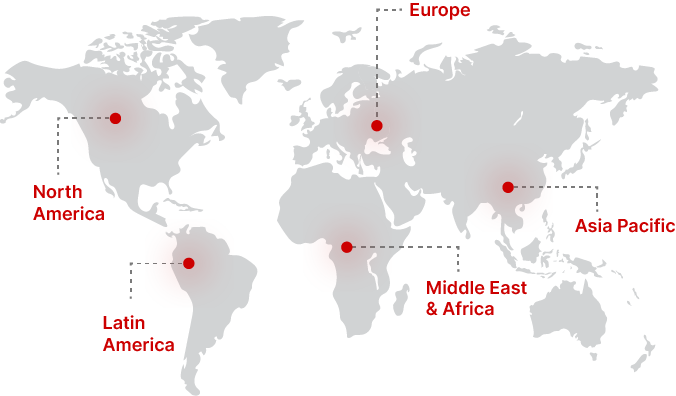
North America
North America accounted for a 35.6% share of the GaN Substrate Wafer Market in 2025 and is expected to grow at a CAGR of 12.8% during the forecast period. The region benefits from strong technological infrastructure and high investments in semiconductor research. The presence of leading electronics manufacturers and defense organizations has contributed to the widespread adoption of GaN technology. Additionally, the increasing demand for advanced communication systems and power electronics is supporting market growth across the region.
The United States remains the dominant country in North America, driven by its robust semiconductor industry and strong focus on innovation. One unique growth factor is the increasing investment in defense and aerospace technologies, where GaN wafers are widely used in radar and communication systems. Government initiatives supporting domestic semiconductor manufacturing have also played a crucial role in boosting market growth.
Europe
Europe held a significant share of the GaN Substrate Wafer Market in 2025 and is projected to grow at a CAGR of 11.9% during the forecast period. The region’s focus on sustainability and energy efficiency has driven the adoption of GaN technology in power electronics and renewable energy applications. Countries across Europe are investing in advanced semiconductor technologies to strengthen their industrial capabilities and reduce dependency on imports.
Germany is the dominant country in this region, supported by its strong automotive industry. A key growth factor is the increasing adoption of electric vehicles and renewable energy systems, which require efficient power management solutions. The integration of GaN wafers in automotive applications is expected to drive further market expansion in the region.
Asia Pacific
Asia Pacific is expected to grow at the fastest CAGR of 14.2% during 2026–2034, driven by rapid industrialization and expanding electronics manufacturing. The region has become a hub for semiconductor production, with countries investing heavily in advanced technologies. The increasing demand for consumer electronics and communication devices is further supporting market growth.
China leads the Asia Pacific market due to its large manufacturing base and government support for semiconductor development. A unique growth factor is the rapid expansion of 5G infrastructure, which has significantly increased demand for GaN-based RF devices. This trend is expected to continue as the country advances its telecommunications capabilities.
Middle East & Africa
The Middle East & Africa region is witnessing steady growth in the GaN Substrate Wafer Market, with a moderate CAGR during the forecast period. The increasing adoption of advanced technologies in telecommunications and energy sectors is driving demand for GaN wafers. Investments in infrastructure development and digital transformation are further supporting market expansion.
The United Arab Emirates is a key contributor to the regional market, driven by its focus on smart city initiatives and advanced communication systems. A unique growth factor is the growing investment in renewable energy projects, where GaN technology is used to enhance power efficiency and performance.
Latin America
Latin America is emerging as a potential market for GaN substrate wafers, with a steady growth rate expected during the forecast period. The region is gradually adopting advanced semiconductor technologies, particularly in telecommunications and industrial applications. Government initiatives to modernize infrastructure are also contributing to market growth.
Brazil dominates the Latin American market, supported by its expanding industrial sector. A unique growth factor is the increasing demand for energy-efficient solutions in industrial applications, which has led to the adoption of GaN-based devices. This trend is expected to continue as industries focus on improving operational efficiency.
Competitive Landscape
The GaN Substrate Wafer Market is characterized by the presence of several established players and emerging companies focusing on technological innovation. Key companies are investing in research and development to improve wafer quality, reduce production costs, and expand their product portfolios. Strategic partnerships and collaborations are common as companies aim to strengthen their market position and address evolving customer requirements.
A leading player in the market is Sumitomo Electric Industries, Ltd., which has a strong presence in GaN wafer manufacturing. The company has recently expanded its production capacity to meet increasing demand from the telecommunications and automotive sectors. Other companies are also focusing on developing advanced wafer technologies to enhance performance and efficiency. The competitive landscape is expected to remain dynamic, with continuous advancements in semiconductor technology driving innovation and growth.
Key Players List
- Sumitomo Electric Industries, Ltd.
- Mitsubishi Chemical Corporation
- Wolfspeed, Inc.
- Kyocera Corporation
- Toshiba Corporation
- Qorvo, Inc.
- NXP Semiconductors N.V.
- STMicroelectronics N.V.
- Infineon Technologies AG
- Samsung Electronics Co., Ltd.
- Nichia Corporation
- Soitec S.A.
- IQE plc
- AXT, Inc.
- GlobalWafers Co., Ltd.
Recent Developments
- Sumitomo Electric Industries expanded its GaN wafer production facility to support increasing demand from 5G and automotive applications.
- Wolfspeed, Inc. announced the development of next-generation GaN-on-SiC wafers with improved thermal performance for RF applications.
- STMicroelectronics partnered with automotive manufacturers to integrate GaN-based power devices into electric vehicle platforms.
GaN Substrate Wafer Market Segments
Type
- Bulk GaN Wafer
- GaN-on-Silicon Wafer
- GaN-on-SiC Wafer
Application
- Power Electronics
- RF Devices
- Optoelectronics
End-Use
- Telecommunications
- Automotive
- Industrial
- Consumer Electronics
- Aerospace & Defense
By Region
- North America
- Europe
- APAC
- Middle East and Africa
- LATAM