Glass Wafer Carrier Market Size, Share, Demand & Growth Analysis Report By Carrier Type (Ultra-Thin Glass Wafer Carriers, Structured Cavity Carriers, Standard Glass Carriers), By Application (Semiconductor Fabrication, MEMS Packaging, Photonics & Optoelectronics, Advanced Packaging), By End-Use (IDMs, Foundries, OSAT Providers, R&D Institutes) With Regional Forecasts, 2026–2034
USD 3950
Market Overview
The Glass Wafer Carrier Market is projected to witness steady expansion, reaching an estimated USD 1.42 billion in 2026 and advancing to approximately USD 2.78 billion by 2034, registering a compound annual growth rate (CAGR) of 8.7% during the forecast period of 2026–2034. Growth in this market is strongly influenced by the rapid scaling of semiconductor fabrication processes, where glass wafer carriers are increasingly adopted for precision handling, ultra-flat support surfaces, and contamination-free wafer transport across advanced nodes.
A key global factor supporting market growth is the accelerating demand for miniaturized and high-performance semiconductor devices used in artificial intelligence hardware, 5G infrastructure, and advanced consumer electronics. The expansion of fabrication plants in Asia Pacific and North America has further strengthened adoption of high-precision wafer handling solutions. Glass wafer carriers, due to their thermal stability and dimensional accuracy, are becoming critical in next-generation lithography and wafer bonding processes.
Key Highlights
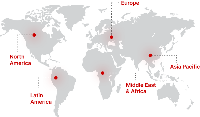
- North America dominated the market with a 34.2% share in 2025.
- Asia Pacific is expected to grow at the fastest CAGR of 11.3% during 2026–2034.
- By carrier type, ultra-thin glass wafer carriers accounted for the largest share of 39.1%.
- while structured cavity carriers are projected to grow at a CAGR of 12.6%.
- By application, semiconductor fabrication led with a 44.3% share.
- whereas MEMS packaging is expected to expand at a CAGR of 11.9%.
- The United States remained the dominant country, with market values of USD 620 million in 2024 and USD 675 million in 2025.
Market Trends
Adoption of Ultra-Thin Glass Wafer Carrier Technologies
The Glass Wafer Carrier Market is experiencing a notable shift toward ultra-thin glass substrates designed for advanced semiconductor nodes below 10nm. These carriers offer superior flatness, reduced particle contamination, and improved thermal stability compared to traditional silicon-based carriers. Manufacturers are increasingly investing in chemical-strengthened glass materials that provide high mechanical durability while maintaining optical transparency for inspection processes. The trend is particularly driven by advanced packaging applications such as fan-out wafer-level packaging and 3D integration, where precision alignment is critical. Additionally, equipment manufacturers are integrating automated handling systems compatible with ultra-thin carriers, further strengthening adoption across high-volume semiconductor fabs globally.
Integration of Smart Monitoring and Metrology Features
Another emerging trend in the Glass Wafer Carrier Market is the integration of embedded monitoring and metrology features within carrier systems. Manufacturers are developing carriers with micro-sensors capable of tracking stress distribution, temperature variations, and surface contamination levels during wafer transport. This enhances process control and reduces defect rates in high-value semiconductor manufacturing. The trend aligns with the broader Industry 4.0 movement, where smart manufacturing systems rely on real-time data acquisition for yield optimization. Semiconductor fabs are increasingly adopting these intelligent carriers to minimize downtime, improve traceability, and enhance quality assurance across multi-step fabrication processes.
Market Drivers
Expansion of Advanced Semiconductor Fabrication Facilities
The rapid global expansion of semiconductor fabrication facilities is a major driver for the Glass Wafer Carrier Market. Governments across the United States, South Korea, Taiwan, and Europe are investing heavily in domestic chip manufacturing to strengthen supply chain resilience. These new fabs require highly precise wafer handling solutions to support next-generation nodes and advanced packaging technologies. Glass wafer carriers offer low thermal expansion and high surface flatness, making them suitable for extreme ultraviolet lithography processes. As semiconductor complexity increases, the need for contamination-free and mechanically stable carriers continues to grow across both logic and memory chip production environments.
Rising Demand for High-Precision Packaging Solutions
The increasing demand for advanced packaging solutions such as system-in-package (SiP) and wafer-level packaging is significantly driving the adoption of glass wafer carriers. These applications require extremely precise alignment and minimal particle interference during wafer stacking and bonding processes. Glass carriers provide superior optical transparency, enabling improved inspection accuracy during automated quality control steps. Furthermore, the shift toward heterogeneous integration of multiple chiplets in a single package is increasing reliance on high-stability carrier systems. This trend is particularly strong in applications such as AI processors, automotive electronics, and high-performance computing systems.
Market Restraint
High Manufacturing Complexity and Cost Constraints
One of the key restraints in the Glass Wafer Carrier Market is the high cost and complexity associated with manufacturing ultra-precision glass carriers. The production process requires advanced chemical strengthening, laser cutting, and surface polishing techniques to achieve nanoscale flatness and defect-free surfaces. These processes significantly increase production costs compared to conventional silicon carriers. Additionally, yield losses during manufacturing due to micro-cracking or warping further elevate operational expenses. Smaller semiconductor equipment suppliers often face challenges in adopting glass carriers due to cost sensitivity, limiting widespread penetration in mid-tier fabrication facilities.
Market Opportunities
Expansion of Heterogeneous Integration and Chiplet Architectures
The growing adoption of heterogeneous integration and chiplet-based semiconductor architectures presents a significant opportunity for the Glass Wafer Carrier Market. These advanced architectures require highly accurate wafer alignment and multi-layer bonding processes, where glass carriers offer superior dimensional stability. As chiplet-based design becomes more prominent in AI processors, data centers, and automotive electronics, demand for high-precision carrier systems is expected to increase. Glass wafer carriers support improved thermal performance and reduced distortion during stacking, making them suitable for next-generation integrated circuit manufacturing environments.
Growth in MEMS and Photonics Applications
Another promising opportunity lies in the expansion of MEMS devices and photonics-based technologies. These applications require ultra-clean processing environments and precise wafer handling systems to maintain device integrity. Glass wafer carriers are increasingly used in MEMS fabrication due to their chemical resistance and optical transparency. In photonics manufacturing, they enable accurate alignment during wafer bonding and lithography processes. The rising deployment of optical sensors, LiDAR systems, and micro-actuators in automotive and industrial applications is expected to further enhance demand for specialized glass carrier solutions.
Segmental Analysis
Carrier Type Segment
Ultra-thin glass wafer carriers accounted for approximately 39.1% share in 2024 within the Glass Wafer Carrier Market. These carriers are widely used in advanced semiconductor fabrication due to their superior flatness, thermal stability, and compatibility with next-generation lithography processes. Their adoption is especially strong in logic chip manufacturing and high-density memory applications, where precision is essential.
Structured cavity carriers are projected to grow at a CAGR of 12.6%, driven by increasing demand in wafer bonding and heterogeneous integration processes. These carriers enable multi-layer stacking with reduced stress and improved alignment accuracy. Their adoption is expanding in advanced packaging applications, particularly in AI and high-performance computing systems.
Application Segment
Semiconductor fabrication led the application segment with approximately 44.3% share in 2024. The dominance is attributed to extensive usage of glass wafer carriers in wafer transport, lithography, and inspection processes. High-volume manufacturing facilities rely heavily on these carriers to ensure process stability and reduce contamination risks.
MEMS packaging is expected to grow at a CAGR of 11.9%, supported by increasing deployment of sensors in automotive, healthcare, and industrial automation applications. Glass wafer carriers provide high optical clarity and chemical resistance, making them suitable for precision MEMS fabrication environments.
End-Use Segment
Integrated device manufacturers accounted for around 41.8% share in 2024, driven by their large-scale semiconductor production requirements. These manufacturers rely on glass wafer carriers for maintaining yield efficiency and ensuring precision in high-volume fabrication environments.
Foundries are projected to grow at a CAGR of 12.1%, supported by rising outsourcing of semiconductor production. Increased demand for advanced nodes and customized chip designs is encouraging foundries to adopt high-performance glass wafer carrier systems.
Regional Analysis
North America
North America accounted for approximately 34.2% share in 2025, with a projected CAGR of 8.5% through 2034 in the Glass Wafer Carrier Market. The region benefits from strong semiconductor R&D capabilities and government-backed initiatives supporting domestic chip manufacturing. Investments in advanced fabrication facilities across the United States continue to drive demand for precision wafer handling systems.
The United States dominates the regional landscape due to its established semiconductor ecosystem and presence of leading fabrication plants. A key growth factor is the expansion of AI and high-performance computing chip production, which requires ultra-precise wafer processing solutions to maintain yield efficiency and reduce contamination risks.
Europe
Europe held around 18.6% market share in 2025, with a CAGR of 8.1% expected through 2034. The region’s growth is supported by increasing investments in automotive semiconductor manufacturing and industrial electronics production. Germany and France are central to regional demand.
Germany leads the European market due to its strong automotive electronics industry. A key growth factor is the rising adoption of advanced driver-assistance systems, which require high-precision semiconductor components produced using glass wafer carrier technologies.
Asia Pacific
Asia Pacific accounted for nearly 32.8% share in 2025, and is projected to grow at the fastest CAGR of 11.3% through 2034. The region benefits from large-scale semiconductor manufacturing hubs and strong supply chain integration.
Taiwan, South Korea, and China are dominant contributors. A key growth factor is the presence of large foundries producing advanced-node chips, which significantly increases the demand for ultra-flat and contamination-free wafer carriers.
Middle East & Africa
The region held approximately 5.4% share in 2025, with a CAGR of 7.9% expected through 2034. Growth is driven by emerging investments in electronics assembly and diversification into semiconductor-related technologies.
Israel leads the region due to its strong semiconductor design ecosystem. A key growth factor is increasing R&D investment in microelectronics and defense-grade semiconductor applications.
Latin America
Latin America accounted for nearly 9% share in 2025, with a CAGR of 8.3% forecast through 2034. Growth is supported by expanding electronics manufacturing and industrial automation adoption.
Brazil dominates the region due to its growing electronics production base. A key growth factor is increasing demand for industrial sensors and automotive electronics supporting regional manufacturing expansion.
Competitive Landscape
The Glass Wafer Carrier Market is moderately consolidated, with key players focusing on material innovation, surface engineering, and precision manufacturing. Companies such as SCHOTT AG, Corning Incorporated, AGC Inc., Nippon Electric Glass, and HOYA Corporation are actively investing in advanced glass substrates for semiconductor applications. SCHOTT AG maintains a strong position due to its extensive portfolio of specialty glass solutions used in wafer processing environments. A recent development includes expansion of high-precision glass fabrication capacity to support next-generation semiconductor demand.
The competitive environment of the Glass Wafer Carrier Market is characterized by a mix of global specialty glass manufacturers and precision semiconductor material suppliers focusing on advanced packaging applications, wafer-level processing, and MEMS fabrication. Companies including SCHOTT AG, Corning Incorporated, AGC Inc., and Nippon Electric Glass Co., Ltd. are strengthening their market positions through investments in ultra-thin glass technologies, high-flatness substrates, and thermal-stability enhancements for semiconductor manufacturing. Competition is increasingly shifting from pricing toward product precision, low total thickness variation, and compatibility with advanced wafer bonding systems. Market participants are also expanding partnerships with foundries and OSAT providers to support growing demand for chiplet integration, fan-out wafer-level packaging, and AI semiconductor applications. Several companies are enhancing regional manufacturing capabilities to improve supply chain resilience and reduce lead times for semiconductor customers.
Key Players
- SCHOTT AG
- Corning Incorporated
- AGC Inc.
- Nippon Electric Glass
- HOYA Corporation
- Plan Optik AG
- Asahi Glass Co.
- Techno Quartz Inc.
- Ohara Inc.
- Kyocera Corporation
- NGK Insulators Ltd.
- Swift Glass Company
- MKS Instruments
- Mitsubishi Materials Corporation
- Saint-Gobain Performance Glass
Recent Developments
- In January 2025, Samsung Electronics announced a strategic collaboration with multiple glass substrate partners to accelerate large-format glass carrier production for advanced semiconductor packaging applications.
- In December 2024, SCHOTT AG expanded its semiconductor-focused operations and allocated additional investment toward precision glass processing facilities in Germany and Singapore to strengthen wafer carrier manufacturing capacity.
- In January 2025, AGC Inc. introduced an ultra-thin 30μm glass substrate designed for fan-out wafer-level packaging and chiplet integration, improving thermal management and dimensional stability for next-generation semiconductor devices.
- LPKF Laser & Electronics expanded its Vitrion platform in 2025 with integrated glass handling systems aimed at semiconductor fabrication facilities using advanced wafer carrier technologies.
Glass Wafer Carrier Market Segments
Carrier Type
- Ultra-Thin Glass Wafer Carriers
- Structured Cavity Carriers
- Standard Glass Carriers
Application
- Semiconductor Fabrication
- MEMS Packaging
- Photonics & Optoelectronics
- Advanced Packaging
End-Use
- Integrated Device Manufacturers (IDMs)
- Foundries
- OSAT Providers
- Research & Development Institutes
By Region
- North America
- Europe
- APAC
- Middle East and Africa
- LATAM