Semiconductor Dielectric Etching Equipment Market Size, Share Demand Report By Type (Plasma Etching, Atomic Layer Etching), By Application (Integrated Circuits, MEMS, Sensors), By End-Use (IDMs, Foundries), By Technology (Reactive Ion Etching, Inductively Coupled Plasma, Others), By Region & Segment Forecasts, 2026–2034
USD 3950
Market Overview
The Semiconductor Dielectric Etching Equipment Market size was valued at approximately USD 9.4 billion in 2026 and is projected to reach USD 17.8 billion by 2034, expanding at a CAGR of 8.3% during the forecast period (2026–2034). The market growth is primarily supported by the global expansion of semiconductor fabrication capacity, driven by rising demand for advanced chips across consumer electronics, automotive, and high-performance computing sectors.
A key global factor accelerating the market is the increasing transition toward advanced process nodes (below 10nm), which requires highly precise dielectric etching technologies to maintain device performance and reliability. Manufacturers are investing in plasma-based etching equipment capable of achieving atomic-level accuracy, further boosting adoption rates.
Key Highlights:
- Asia Pacific dominated the market with 48.6% share in 2025, while North America is expected to register the fastest growth at a CAGR of 9.1%.
- Plasma etching equipment emerged as the leading subsegment with 63.4% share, while atomic layer etching is projected to grow at a CAGR of 10.2%.
- Integrated device manufacturers (IDMs) led the end-use segment with 54.7% share, whereas foundries are expected to grow fastest at 9.5% CAGR.
- The United States recorded market values of USD 2.1 billion in 2024 and USD 2.3 billion in 2025, reflecting steady technological investments.
Market Trends
Increasing Adoption of Atomic Layer Etching (ALE) Technologies
The Semiconductor Dielectric Etching Equipment Market is witnessing a shift toward atomic layer etching (ALE) as chip manufacturers demand higher precision and control at nanoscale levels. ALE enables layer-by-layer material removal, improving uniformity and reducing defects. This trend is particularly relevant for advanced nodes such as 5nm and 3nm, where traditional plasma etching methods face limitations. Equipment manufacturers are integrating ALE capabilities into existing platforms, enhancing process flexibility and efficiency. As semiconductor designs become more complex, ALE is expected to play a critical role in enabling next-generation device architectures.
Integration of AI and Process Automation in Etching Systems
Another significant trend shaping the market is the integration of artificial intelligence (AI) and advanced automation in etching equipment. AI-driven process control systems allow real-time monitoring and optimization of etching parameters, improving yield and reducing downtime. Semiconductor fabrication facilities are increasingly adopting smart manufacturing practices to enhance productivity and reduce operational costs. Automated etching systems also support predictive maintenance, minimizing equipment failure and extending lifecycle. This trend is expected to accelerate as fabs prioritize efficiency and scalability in high-volume production environments.
Market Drivers
Rising Demand for Advanced Semiconductor Devices
The growing demand for high-performance semiconductor devices across industries such as consumer electronics, automotive, and telecommunications is a major driver for the Semiconductor Dielectric Etching Equipment Market. Advanced applications including 5G networks, artificial intelligence, and electric vehicles require chips with higher density and improved functionality. This has led to increased investments in semiconductor manufacturing facilities and advanced fabrication technologies, thereby boosting demand for dielectric etching equipment.
Expansion of Global Semiconductor Manufacturing Capacity
Governments and private players are investing heavily in expanding semiconductor manufacturing capacity to reduce supply chain dependencies and meet rising demand. New fabrication plants and capacity expansions are driving the need for advanced etching equipment. Countries across Asia Pacific, North America, and Europe are implementing supportive policies and incentives to strengthen domestic semiconductor production. This expansion is expected to significantly contribute to market growth over the forecast period.
Market Restraint
High Capital Investment and Maintenance Costs
One of the major challenges in the Semiconductor Dielectric Etching Equipment Market is the high capital investment required for advanced etching systems. These systems involve sophisticated technologies, including plasma generation, vacuum chambers, and precision control mechanisms, making them expensive to acquire and maintain. Small and medium-sized semiconductor manufacturers may find it difficult to invest in such high-cost equipment, limiting market penetration.
Additionally, maintenance costs and the need for skilled personnel to operate these systems add to the overall operational expenses. Frequent upgrades are also necessary to keep pace with evolving semiconductor technologies, further increasing the financial burden on manufacturers. These factors may hinder market growth, particularly in developing regions where access to capital and technical expertise is limited.
Market Opportunities
Growth in 3D NAND and Advanced Memory Technologies
The increasing adoption of 3D NAND and other advanced memory technologies presents significant opportunities for the Semiconductor Dielectric Etching Equipment Market. These technologies require complex etching processes to create high-aspect-ratio structures, driving demand for specialized equipment. As data storage needs continue to grow, manufacturers are investing in advanced memory solutions, creating new growth avenues for etching equipment providers.
Emerging Semiconductor Markets in Developing Economies
Developing economies are emerging as potential growth markets for semiconductor manufacturing, supported by government initiatives and foreign investments. Countries in Southeast Asia, the Middle East, and Latin America are focusing on building semiconductor ecosystems to reduce reliance on imports. This expansion is expected to create demand for dielectric etching equipment, offering opportunities for market players to expand their global footprint.
Segmental Analysis
By Type
Plasma etching equipment dominated the Semiconductor Dielectric Etching Equipment Market with a 63.4% share in 2025, owing to its widespread use in semiconductor fabrication processes. It offers high precision and efficiency, making it suitable for advanced manufacturing requirements.
Atomic layer etching is expected to be the fastest-growing subsegment, with a projected CAGR of 10.2%, driven by its ability to achieve atomic-scale precision and support advanced node manufacturing.
By Application
Integrated circuits accounted for the largest share of 58.1% in 2025, as dielectric etching is essential in IC fabrication processes. The increasing complexity of IC designs has further boosted demand.
MEMS applications are expected to grow at a CAGR of 9.4%, supported by rising demand for sensors and microdevices in automotive and consumer electronics sectors.
By End-Use
Integrated device manufacturers (IDMs) dominated the market with a 54.7% share in 2025, driven by their extensive in-house manufacturing capabilities.
Foundries are expected to grow at the fastest CAGR of 9.5%, as outsourcing of semiconductor manufacturing continues to increase globally.
By Technology
Reactive ion etching (RIE) held a significant share of 49.3% in 2025, owing to its ability to provide anisotropic etching for complex structures.
Inductively coupled plasma (ICP) technology is projected to grow at a CAGR of 9.8%, driven by its superior control and efficiency in advanced applications.
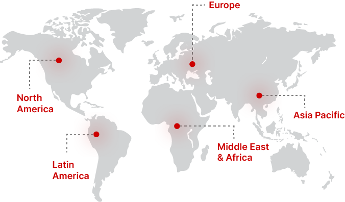
Regional Analysis
North America
North America accounted for 21.8% of the Semiconductor Dielectric Etching Equipment Market share in 2025 and is projected to grow at a CAGR of 9.1% during the forecast period. The region's growth is driven by strong investments in semiconductor R&D and manufacturing infrastructure.
The United States dominated the regional market due to its advanced semiconductor ecosystem and focus on technological innovation. The presence of leading chip manufacturers and equipment suppliers has supported steady market expansion.
Europe
Europe held 16.4% market share in 2025 and is expected to grow at a CAGR of 7.6% from 2026 to 2034. The region is focusing on strengthening its semiconductor supply chain and reducing dependency on imports.
Germany emerged as the dominant country, supported by its robust industrial base and investments in semiconductor manufacturing technologies. Government initiatives aimed at boosting domestic production have further contributed to market growth.
Asia Pacific
Asia Pacific led the market with a 48.6% share in 2025 and is expected to grow at a CAGR of 8.7% during the forecast period. The region remains the global hub for semiconductor manufacturing, driven by strong demand and large-scale production facilities.
China dominated the regional market, supported by significant investments in semiconductor fabrication and government-backed initiatives. The country's focus on self-sufficiency in semiconductor production has accelerated demand for etching equipment.
Middle East & Africa
The Middle East & Africa accounted for 6.2% of the market share in 2025 and is projected to grow at a CAGR of 7.9%. The region is gradually expanding its presence in the semiconductor industry through strategic investments.
The United Arab Emirates emerged as the leading country, driven by initiatives to diversify its economy and invest in high-tech industries. Infrastructure development and partnerships with global players are supporting market growth.
Latin America
Latin America held 7.0% market share in 2025 and is expected to grow at a CAGR of 7.3% during the forecast period. The region is witnessing gradual adoption of semiconductor technologies across industries.
Brazil dominated the regional market due to its growing electronics manufacturing sector and increasing investments in technology infrastructure. The country's focus on industrial development is expected to drive demand for etching equipment.
Competitive Landscape
The Semiconductor Dielectric Etching Equipment Market is moderately consolidated, with key players focusing on innovation and strategic partnerships to strengthen their market position. Leading companies are investing in advanced technologies such as atomic layer etching and AI-driven process optimization.
A prominent market leader is Lam Research Corporation, which continues to expand its product portfolio through technological advancements. The company recently introduced next-generation etching systems designed for advanced nodes, enhancing process efficiency and precision.
Other major players are also focusing on expanding their global presence and improving service capabilities to cater to evolving customer demands.
Key Players List
- Lam Research Corporation
- Applied Materials, Inc.
- Tokyo Electron Limited
- Hitachi High-Tech Corporation
- ASM International
- KLA Corporation
- Plasma-Therm LLC
- Oxford Instruments plc
- SPTS Technologies Ltd.
- ULVAC, Inc.
- EV Group
- SAMCO Inc.
- NAURA Technology Group Co., Ltd.
- AMEC (Advanced Micro-Fabrication Equipment Inc.)
- Canon Anelva Corporation
Recent Developments
- 2025: Lam Research introduced advanced dielectric etching systems for sub-5nm nodes.
- 2025: Applied Materials expanded its etching equipment portfolio with AI-enabled solutions.
- 2024: Tokyo Electron launched next-generation plasma etching tools for high-volume manufacturing.
- 2024: Hitachi High-Tech invested in R&D for advanced semiconductor fabrication technologies.
- 2023: ASM International enhanced its etching capabilities through strategic collaborations.
Semiconductor Dielectric Etching Equipment Market Segments
Type
- Plasma Etching
- Atomic Layer Etching
Application
- Integrated Circuits
- MEMS
- Sensors
End-Use
- Integrated Device Manufacturers (IDMs)
- Foundries
Technology
- Reactive Ion Etching
- Inductively Coupled Plasma
- Others
By Region
- North America
- Europe
- APAC
- Middle East and Africa
- LATAM