Semiconductor Polishing Pad Market Size, Share Demand Report By Type (Polyurethane Pads, Non-Polyurethane Pads, Fixed Abrasive Pads), By Application (Wafer Polishing, Advanced Node Fabrication, MEMS and Sensors), By End-Use (Integrated Device Manufacturers, Foundries, OSAT Companies) By Region & Segment Forecasts, 2026–2034
USD 3950
Market Overview
The Semiconductor Polishing Pad Market size is projected to reach a valuation of approximately USD 2.85 billion in 2026 and is expected to grow to around USD 5.62 billion by 2034, registering a compound annual growth rate (CAGR) of 8.9% during the forecast period. This growth trajectory is primarily supported by the rapid expansion of advanced semiconductor fabrication technologies, particularly in logic and memory devices. The increasing adoption of artificial intelligence, high-performance computing, and 5G infrastructure has significantly boosted wafer production volumes, thereby driving demand for chemical mechanical planarization (CMP) consumables such as polishing pads.
A major global factor contributing to market growth is the scaling of semiconductor nodes below 7nm, which requires higher precision and defect-free surfaces. Polishing pads play a critical role in achieving uniform wafer surfaces, making them indispensable in semiconductor manufacturing. As chipmakers focus on improving yield and reducing defects, the importance of high-performance polishing pads continues to rise.
Key Highlights
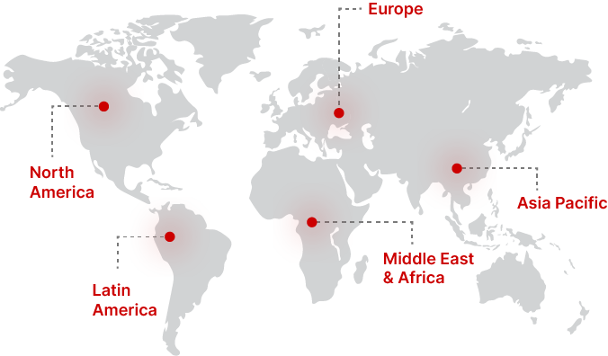
- North America dominated the market with a 33.8% share in 2025.
- Asia Pacific is expected to grow at the fastest CAGR of 10.7% during 2026–2034.
- By type, polyurethane pads accounted for the largest share of 46.3%, while fixed abrasive pads are projected to grow at a CAGR of 9.8%.
- By application, wafer polishing led with a 52.1% share, whereas advanced node fabrication is expected to expand at a CAGR of 10.3%.
- The United States remained the dominant country, with market values of USD 620 million in 2024 and USD 675 million in 2025.
Market Trends
Increasing Adoption of Advanced CMP Technologies
The semiconductor industry is witnessing a steady shift toward advanced chemical mechanical planarization technologies, which is shaping the demand for high-performance polishing pads. As chip manufacturers move toward smaller node sizes, the complexity of wafer surfaces increases significantly, requiring more precise planarization processes. This has led to the development of multi-layer polishing techniques that rely on pads with enhanced durability, uniformity, and consistency. Manufacturers are focusing on optimizing pad porosity and hardness to ensure better slurry distribution and defect minimization. Additionally, the integration of automation in fabrication plants is increasing the need for pads that offer predictable performance over extended cycles, further strengthening this trend.
Rising Demand from Emerging Semiconductor Applications
Emerging applications such as artificial intelligence processors, electric vehicles, and IoT devices are contributing to increased semiconductor production, thereby influencing polishing pad demand. These applications require high-performance chips with minimal defects, driving the need for efficient polishing solutions. Moreover, the transition toward heterogeneous integration and 3D packaging technologies is creating additional layers in semiconductor devices, increasing the number of polishing steps required. This trend is encouraging manufacturers to develop specialized pads tailored for different materials and layers. As innovation continues across end-use industries, the demand for advanced polishing pads is expected to remain strong.
Market Drivers
Expansion of Semiconductor Manufacturing Capacity
The global expansion of semiconductor manufacturing facilities is a key driver of the polishing pad market. Governments and private companies are investing heavily in new fabrication plants to address supply chain disruptions and meet rising demand for chips. These new facilities require a steady supply of CMP consumables, including polishing pads, to maintain production efficiency. The growing emphasis on domestic semiconductor production in regions such as North America and Europe is further accelerating investments. As fabrication capacity increases, the consumption of polishing pads rises proportionally, making this a significant growth driver for the market.
Growing Importance of Yield Enhancement and Defect Reduction
Semiconductor manufacturers are increasingly focused on improving yield rates and minimizing defects during production. Polishing pads play a crucial role in achieving uniform wafer surfaces, which directly impacts device performance and reliability. Even minor imperfections can lead to significant losses in yield, prompting manufacturers to invest in high-quality polishing solutions. Advanced pads with improved material properties help reduce defects such as scratches and dishing. As competition intensifies in the semiconductor industry, the need for efficient and reliable polishing processes is becoming more critical, thereby driving demand for innovative polishing pad technologies.
Market Restraint
High Cost and Frequent Replacement Requirements
One of the primary restraints affecting the Semiconductor Polishing Pad Market is the high cost associated with these consumables and their frequent replacement during manufacturing processes. Polishing pads experience wear and tear due to continuous use in abrasive environments, leading to reduced performance over time. This necessitates regular replacement, increasing operational costs for semiconductor manufacturers. Smaller fabrication facilities may face challenges in managing these expenses, particularly in highly competitive markets where cost optimization is essential. Additionally, the need for precise calibration and compatibility with specific slurry formulations adds complexity to procurement decisions. These factors collectively limit market growth, especially in cost-sensitive regions.
Market Opportunities
Development of Environmentally Sustainable Polishing Pads
The growing emphasis on sustainability presents a significant opportunity for the polishing pad market. Semiconductor manufacturers are seeking eco-friendly solutions that reduce environmental impact without compromising performance. This has led to research into biodegradable materials and recyclable pad designs. Companies that invest in sustainable product development can gain a competitive advantage by aligning with regulatory requirements and customer preferences. Furthermore, reducing waste generated during the CMP process can lower overall operational costs, making sustainable pads an attractive option for manufacturers aiming to improve efficiency and environmental compliance.
Advancements in Material Science and Customization
Innovations in material science are opening new avenues for the development of customized polishing pads tailored to specific applications. Advanced materials with improved durability, uniformity, and chemical resistance are enhancing pad performance. Customization allows manufacturers to optimize pads for different wafer types, including silicon, compound semiconductors, and advanced packaging structures. This flexibility is particularly valuable in modern fabrication processes that involve multiple layers and materials. As semiconductor technologies continue to evolve, the demand for specialized polishing solutions is expected to increase, creating growth opportunities for market players.
Segmental Analysis
By Type
Polyurethane polishing pads dominated the Semiconductor Polishing Pad Market, accounting for approximately 46.3% of the market share in 2024. These pads are widely used due to their excellent durability, flexibility, and compatibility with various slurry formulations. Their ability to provide uniform pressure distribution across the wafer surface makes them suitable for a wide range of applications. Additionally, polyurethane pads offer consistent performance over extended usage cycles, reducing the frequency of replacements. This has made them the preferred choice among semiconductor manufacturers aiming to optimize production efficiency and maintain high-quality standards.
Fixed abrasive pads are expected to be the fastest-growing subsegment, registering a CAGR of 9.8% during the forecast period. These pads incorporate abrasive particles within their structure, eliminating the need for slurry in certain applications. This results in improved process control and reduced waste generation. The growing focus on sustainability and cost efficiency is driving the adoption of fixed abrasive pads. Their ability to deliver consistent material removal rates and minimize defects makes them increasingly popular in advanced semiconductor fabrication processes.
By Application
Wafer polishing emerged as the dominant application segment, accounting for a 52.1% share in 2024. This segment includes the planarization of silicon wafers during various stages of semiconductor manufacturing. The increasing complexity of semiconductor devices has led to a higher number of polishing steps, driving demand for high-performance pads. Wafer polishing is critical for achieving smooth and defect-free surfaces, which are essential for device functionality. As semiconductor manufacturers continue to scale down node sizes, the importance of efficient polishing processes remains significant.
Advanced node fabrication is projected to be the fastest-growing application segment, with a CAGR of 10.3% during the forecast period. The transition to smaller nodes requires precise control over surface topography, increasing the demand for specialized polishing pads. These pads are designed to handle complex materials and multi-layer structures, ensuring optimal performance. The growing adoption of technologies such as artificial intelligence and high-performance computing is driving demand for advanced semiconductor devices, thereby supporting the growth of this segment.
By End-Use
Integrated device manufacturers (IDMs) dominated the end-use segment, accounting for a significant share of the market in 2024. These companies handle both the design and manufacturing of semiconductor devices, requiring a steady supply of CMP consumables. IDMs prioritize quality and consistency in their production processes, making them major consumers of polishing pads. Their large-scale operations and continuous investments in advanced fabrication technologies further contribute to their dominant position in the market.
Foundries are expected to be the fastest-growing end-use segment, with a CAGR of 9.5% during the forecast period. Foundries specialize in manufacturing semiconductor devices for other companies, leading to high production volumes. The increasing demand for outsourced semiconductor manufacturing is driving the growth of this segment. Foundries require efficient and reliable polishing solutions to meet the diverse needs of their clients. This is encouraging the adoption of advanced polishing pads that offer improved performance and flexibility.
Regional Analysis
North America
North America accounted for approximately 33.8% of the global Semiconductor Polishing Pad Market share in 2025 and is expected to grow at a CAGR of 7.9% during the forecast period. The region benefits from a strong presence of semiconductor manufacturers and technology companies. Continuous investments in research and development, coupled with government initiatives to boost domestic chip production, are supporting market growth. The demand for advanced semiconductor devices in sectors such as aerospace, defense, and healthcare further contributes to the steady expansion of the polishing pad market in this region.
The United States remains the dominant country in North America, driven by its advanced semiconductor ecosystem and innovation capabilities. A unique growth factor is the increasing investment in next-generation fabrication facilities aimed at reducing reliance on imports. These facilities require high-quality CMP consumables, including polishing pads, to achieve optimal production efficiency. The focus on technological leadership and supply chain resilience continues to drive demand in the U.S. market.
Europe
Europe held a market share of around 21.6% in 2025 and is projected to grow at a CAGR of 7.5% through 2034. The region’s semiconductor industry is expanding steadily, supported by initiatives aimed at strengthening local manufacturing capabilities. Increasing demand for automotive electronics and industrial automation is driving the need for semiconductors, thereby boosting the demand for polishing pads. Additionally, collaborations between research institutions and industry players are fostering innovation in CMP technologies.
Germany is the leading country in the European market, benefiting from its strong industrial base and focus on automotive electronics. A unique growth factor in Germany is the rising adoption of electric vehicles, which require advanced semiconductor components. This demand is encouraging semiconductor manufacturers to enhance production capabilities, thereby increasing the need for high-performance polishing pads.
Asia Pacific
Asia Pacific dominated the global market growth outlook and is expected to register the fastest CAGR of 10.7% during the forecast period, with a 2025 share of approximately 29.4%. The region is home to major semiconductor manufacturing hubs, including countries such as China, South Korea, Japan, and Taiwan. Rapid industrialization and increasing demand for consumer electronics are driving semiconductor production, which in turn fuels demand for polishing pads.
China stands out as the dominant country in Asia Pacific due to its aggressive expansion of semiconductor manufacturing capacity. A unique growth factor is the government’s strategic focus on achieving self-sufficiency in semiconductor production. This has led to significant investments in fabrication plants and related technologies, creating substantial demand for CMP consumables, including polishing pads.
Middle East & Africa
The Middle East & Africa region accounted for approximately 7.2% of the market share in 2025 and is expected to grow at a CAGR of 6.8% during the forecast period. Although the semiconductor industry in this region is still developing, increasing investments in technology infrastructure are supporting growth. The adoption of digital technologies and smart city initiatives is driving demand for semiconductors, indirectly boosting the polishing pad market.
The United Arab Emirates is emerging as a key country in the region, driven by its focus on technological innovation and diversification of the economy. A unique growth factor is the increasing investment in data centers and advanced electronics, which require semiconductor components. This trend is expected to support the gradual expansion of the polishing pad market in the region.
Latin America
Latin America held a market share of around 8.0% in 2025 and is projected to grow at a CAGR of 6.5% during the forecast period. The region’s semiconductor market is supported by growing demand for consumer electronics and telecommunications infrastructure. While manufacturing capabilities are limited compared to other regions, increasing imports and assembly operations are contributing to the demand for polishing pads.
Brazil is the dominant country in Latin America, driven by its expanding electronics industry. A unique growth factor is the rising adoption of digital technologies across various sectors, including healthcare and education. This is increasing the demand for semiconductor devices, which in turn supports the growth of the polishing pad market.
Competitive Landscape
The Semiconductor Polishing Pad Market is characterized by the presence of several established players competing on the basis of product quality, innovation, and pricing. Leading companies are focusing on developing advanced materials and customized solutions to meet the evolving requirements of semiconductor manufacturers. Strategic partnerships and collaborations are also common, enabling companies to expand their market presence and enhance technological capabilities.
A prominent leader in the market is Cabot Microelectronics Corporation, known for its extensive portfolio of CMP consumables. The company has recently introduced advanced polishing pads designed for next-generation semiconductor nodes, focusing on improving efficiency and reducing defects. Other key players are investing in research and development to create innovative products that address the challenges associated with modern semiconductor fabrication processes.
Key Players
- Cabot Microelectronics Corporation
- DuPont
- Fujibo Holdings Inc.
- 3M Company
- JSR Corporation
- Entegris Inc.
- SKC Co., Ltd.
- IVT Technologies Co., Ltd.
- KC Tech Co., Ltd.
- TWI Incorporated
- FNS TECH Co., Ltd.
- Ace Nanochem Co., Ltd.
- Dongjin Semichem Co., Ltd.
- Nitta Haas Incorporated
- Asahi Glass Co., Ltd.
Recent Developments
- Several companies have introduced advanced polishing pad materials designed for sub-5nm semiconductor nodes, focusing on improved durability and uniformity.
- Strategic collaborations between polishing pad manufacturers and semiconductor companies have increased, aiming to develop customized solutions for specific fabrication processes.
- Investments in sustainable manufacturing practices have led to the development of eco-friendly polishing pads, reducing environmental impact and improving operational efficiency.
Semiconductor Polishing Pad Market Segments
Type
- Polyurethane Pads
- Non-Polyurethane Pads
- Fixed Abrasive Pads
Application
- Wafer Polishing
- Advanced Node Fabrication
- MEMS and Sensors
End-Use
- Integrated Device Manufacturers (IDMs)
- Foundries
- OSAT Companies
By Region
- North America
- Europe
- APAC
- Middle East and Africa
- LATAM