Semiconductor Seals Market Size, Share & Trends Analysis Report By Material (FFKM, FKM, PTFE & Fluoropolymer, Other Elastomers & Specialty Materials), By Seal Type (O-Rings, Slit Valve & Door Seals, Bonded & Custom Seals, Dynamic & Rotary Seals, Other Seals), By Process (Etching & Cleaning, Deposition, Lithography, CMP, Wet Processing, Other Semiconductor Processes) and By Region (North America, Europe, APAC, Middle East and Africa, LATAM) Forecasts, 2026–2034
USD 3950
Semiconductor Seals Market Size
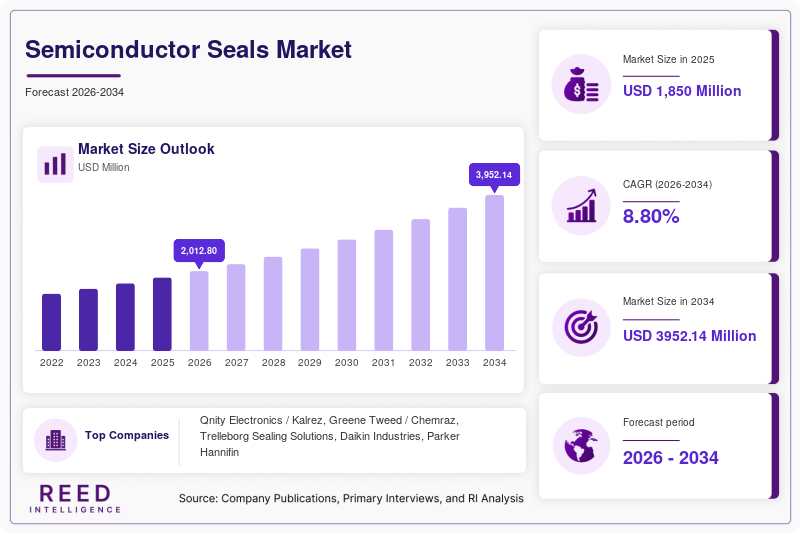
The global semiconductor seals market is valued at USD 1,850 Million in 2025 and USD 2,012.80 Million in 2026. The market is projected to reach USD 3,952.14 Million by 2034, registering an 8.80% CAGR during the forecast period.
The semiconductor seals market comprises high-performance elastomeric, fluoropolymer and engineered sealing components used throughout semiconductor manufacturing equipment to preserve vacuum integrity, isolate process gases and chemicals, limit particle generation, minimize outgassing and protect equipment from aggressive plasma and thermal environments.
The market is particularly important in front-end wafer-processing equipment, where seals can be exposed to fluorine-, chlorine- and oxygen-based plasmas, high-temperature process gases, wet chemicals, vacuum conditions and repeated chamber maintenance cycles. Trelleborg's semiconductor portfolio includes FFKM, FKM and PTFE-based materials for deposition, etching, ash/strip, plasma cleaning and thermal processing, while Precision Polymer Engineering identifies extreme heat, aggressive plasma chemistries, hot wet chemicals and remote NF3 cleaning among the environments that semiconductor elastomer seals must withstand.
Semiconductor Seals Market Drivers
AI-driven semiconductor capacity expansion is increasing demand for high-performance sealing components
The strongest structural demand driver is the continued expansion of wafer-fabrication and advanced-packaging capacity.
SEMI's July 2026 forecast projects global semiconductor manufacturing equipment sales of USD 165.9 Billion in 2026, with wafer-fab equipment accounting for USD 143.9 Billion. Foundry and logic equipment spending is projected to increase 18.9% in 2026, driven by advanced-node capacity for AI accelerators, high-performance computing and premium mobile processors.
This matters for seals because virtually every new or expanded process tool requires qualified sealing components. Etch chambers, deposition chambers, load locks, gas-delivery interfaces, slit valves, vacuum flanges and thermal-processing equipment all depend on sealing performance.
The impact is amplified at advanced nodes because process conditions can become more aggressive and process tolerances narrower. Greene Tweed notes that advanced semiconductor processes demand resistance to aggressive plasma chemistries, elevated temperatures and vacuum conditions while limiting particulate contamination.
As equipment installations increase, the installed base of seals rises through both initial equipment production and recurring replacement cycles.
Advanced nodes and increasingly aggressive process chemistries are raising the performance specification for seals
The semiconductor industry is moving toward smaller process geometries, more complicated transistor structures, higher-aspect-ratio etching, advanced deposition, more intensive cleaning and increased use of complex three-dimensional packaging.
Trelleborg's PureFab portfolio is designed for deposition processes such as PECVD, HDPCVD and PEALD, etching processes including ALE and dry etching, and high-temperature processes such as RTP, ALD, CVD and diffusion furnaces.
Precision Polymer Engineering similarly describes its Perlast, Kimura and Nanofluor families around plasma, thermal and wet-chemical semiconductor applications, with particular emphasis on particle generation, trace-metal contamination and chemical erosion.
This process intensification favors premium FFKM and engineered seals because standard elastomers can degrade more quickly under higher plasma intensity, temperature and chemical exposure.
Yield protection and equipment uptime are increasing the economic value of longer-life seals
The cost of a semiconductor-equipment failure is not limited to the replacement component. A damaged seal can cause a leak, particle event or chamber contamination that leads to tool downtime and potentially affects wafer yield.
Trelleborg states that its high-purity PureFab materials are designed to extend service life, reduce particle generation and increase process-tool uptime. Greene Tweed likewise links high-performance Chemraz solutions to reduced downtime and improved semiconductor yields.
This creates an economic preference for seals evaluated by total cost of ownership rather than purchase price alone. A more expensive seal may remain attractive when it extends preventive-maintenance intervals and lowers the probability of unplanned tool intervention.
The recurring nature of semiconductor equipment maintenance also creates a stable replacement market. Once a material is qualified on a specific tool, replacement demand can continue for the service life of the equipment.
Semiconductor Seals Market Restraints
Semiconductor qualification requirements create long replacement cycles and high barriers to entry
A sealing material used in a production semiconductor tool must demonstrate compatibility with the specific process environment. Factors can include temperature, plasma chemistry, compression set, outgassing, trace-metal contamination, particle generation, dimensional stability and mechanical durability.
Trelleborg maintains extensive semiconductor material-testing and cleanroom manufacturing capabilities, while Precision Polymer Engineering conducts in-house material testing for purity, plasma resistance and high-temperature performance.
Because changing a qualified material can introduce process risk, fabs and equipment manufacturers may be reluctant to switch suppliers without substantial validation. This favors suppliers with long qualification histories and established OEM relationships.
Specialty FFKM supply chains remain material- and process-intensive
Advanced semiconductor-grade FFKM requires specialized polymer chemistry, compounding, molding, post-curing, cleaning, inspection and packaging controls. The supply chain is therefore more complex than that of commodity elastomer products.
Greene Tweed has previously highlighted the sensitivity of high-performance FFKM supply chains to ingredient availability and the effect of semiconductor-demand surges on material supply.
The requirement for ultra-high purity and specific process compatibility also limits the number of suppliers capable of delivering qualified grades at scale.
Semiconductor Seals Market Opportunities
Fluorosurfactant-free and lower-PFAS semiconductor seals are opening a new product-qualification cycle
Environmental requirements are creating opportunities for seal manufacturers to develop next-generation formulations that avoid intentionally added fluorosurfactants while retaining the performance required by advanced fabs.
Trelleborg's August 2026 launch added JPF50, JPF58 and VPF20 to its PureFab portfolio. JPF50 and JPF58 are high-temperature FFKMs, while VPF20 is a high-purity FKM intended for applications where FFKM performance is unnecessary. Trelleborg positions the materials for deposition, etch, RTP, ALD, CVD, diffusion, load locks, EFEMs and vacuum-handling applications.
Daikin is also introducing fluorosurfactant-free manufacturing processes as part of its new Kashima FFKM facility.
This transition creates an opportunity for suppliers to replace existing qualified grades while helping fabs reduce regulatory and supply-chain risk.
Advanced packaging and HBM manufacturing can expand the sealing opportunity beyond conventional front-end equipment
AI computing is increasing demand for high-bandwidth memory and advanced packaging, creating additional process-tool requirements.
SEMI forecasts 2026 equipment growth in advanced memory and packaging and specifically identifies the increasing complexity of AI and HBM devices as a major investment driver.
Greene Tweed's March 2026 analysis states that advanced packaging introduces new materials, temperature tolerances and gas chemistries that create additional sealing challenges across etch, deposition, clean and CMP.
This creates opportunities for custom molded seals, high-temperature FFKM, low-particle compounds and engineered components designed specifically around next-generation packaging tools.
Regionalized manufacturing can improve supply security for fabs and equipment OEMs
The concentration of semiconductor production in Asia and the simultaneous push for regional manufacturing are encouraging seal suppliers to expand production close to semiconductor clusters.
Trelleborg's August 2026 Malta expansion adds more than 500 square meters of cleanroom space and focuses on FKM and FFKM for semiconductor customers, creating a European manufacturing hub alongside its semiconductor-focused operations in the UK and South Korea.
Daikin's Kashima expansion strengthens Japanese production, while major suppliers maintain operations across North America, Europe and Asia. These investments create an opportunity to reduce lead times and mitigate supply-chain disruption risks.
Material Analysis
FFKM remains both the dominant and fastest-growing material as advanced fabs prioritize chemical resistance and ultra-high purity
FFKM remains the central material class for semiconductor sealing because it combines broad chemical resistance with high-temperature capability and low contamination performance.
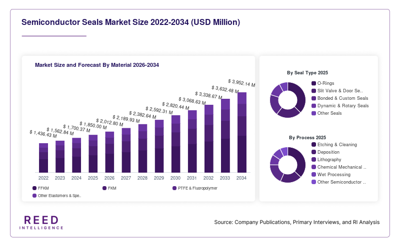
The FFKM segment accounts for 61% of the global market in 2026 and is projected to register a 9.40% CAGR, making it both the dominant and fastest-growing material category.
Qnity's Kalrez portfolio includes perfluoroelastomer components for critical semiconductor manufacturing, while Trelleborg's PureFab FFKM products target aggressive plasma, deposition, etching and thermal-processing environments. Precision Polymer Engineering likewise identifies FFKM as its principal high-performance semiconductor sealing material.
The expansion is being supported by higher process temperatures, more aggressive plasmas and tighter contamination limits.
FKM remains important in lower-temperature and less chemically aggressive semiconductor equipment
The segment is projected to register a 7.20% CAGR.
High-purity FKM provides a lower-cost alternative where temperatures and chemical exposure do not justify FFKM. Trelleborg's VPF20, introduced in 2026, targets transfer modules, load locks, EFEMs, vacuum handling and other purity-critical applications where standard FKM contamination characteristics may be insufficient.
Seal Type Analysis
O-Rings retain the dominant seal-type share because they provide broad compatibility across chambers, valves and vacuum interfaces
O-rings represent the largest installed base because they can be manufactured in many cross-sections and dimensions and incorporated into chamber lids, flanges, gas inlets, load locks, vacuum systems and process modules.
The O-Rings segment accounts for 58% of the global market in 2026 and is projected to register an 8.10% CAGR.
Trelleborg offers semiconductor O-rings from micro to giant sizes and provides both standard and custom products, while PPE manufactures high-purity O-rings for semiconductor fabs, foundries and equipment OEMs.
Slit Valve & Door Seals are the fastest-growing major seal category as wafer-transfer systems become more demanding
The Slit Valve & Door Seals segment accounts for 18% of the global market in 2026 and is projected to register a 10.20% CAGR, making it the fastest-growing major seal category.
Slit-valve seals operate in highly demanding environments where they must combine low particle generation, plasma resistance and mechanical reliability with repeated cycling.
PPE specifically supplies slit-valve door designs using high-purity elastomers, while Trelleborg's JPF50 is identified for bonded slit-valve door applications.
Bonded & Custom Seals are expanding as equipment geometries become more specialized
The segment is projected to register a 9.10% CAGR.
Custom gaskets, molded parts and bonded seals are increasingly important where standard O-rings cannot meet complex geometry, installation or process requirements.
Trelleborg offers custom-designed semiconductor components including gaskets, wafer-handling pads and bonded products, while its FlexiMold platform supports large semiconductor O-rings and specialty geometries.
Process Analysis
Etching & Cleaning remains the dominant process application because plasma and chemical exposure create high seal-consumption requirements
The Etching & Cleaning segment accounts for 39% of the global market in 2026 and is projected to register an 8.60% CAGR.
Dry etching and plasma cleaning expose seals to aggressive chemistries and high-energy plasma. Greene Tweed specifically designs semiconductor sealing solutions for oxygen plasma and aggressive plasma chemistry, while Trelleborg's PureFab range targets dry etching, ALE, ash/strip and plasma-cleaning processes.
Frequent chamber maintenance and the need to control particle generation make seal performance particularly important in these processes.
Deposition is the fastest-growing major process application as advanced thin-film and 3D structures increase process intensity
The Deposition segment accounts for 24% of the global market in 2026 and is projected to register a 9.60% CAGR, making it the fastest-growing major process category.
Trelleborg identifies PECVD, HDPCVD, PEALD, ALD, CVD and diffusion as important semiconductor sealing environments, while Greene Tweed supports deposition-related applications through its broader semiconductor sealing portfolio.
Increasing adoption of advanced deposition techniques for complex transistor structures, memory and advanced packaging is increasing the need for high-temperature, low-outgassing and high-purity seals.
Semiconductor Seals Market Regional Analysis
APAC Semiconductor Seals Market
APAC remains the dominant and fastest-growing regional market because it combines the highest concentration of wafer-fabrication capacity with major semiconductor equipment, materials and packaging ecosystems.
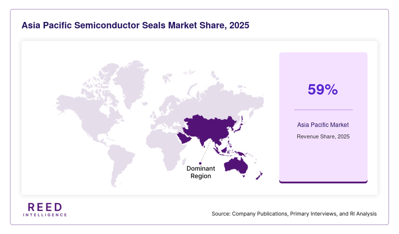
The APAC region accounts for 59% of the global market in 2026 and is projected to register a 10.20% CAGR, making it the fastest-growing regional market.
SEMI reported that China, Taiwan and Korea together accounted for 79% of global semiconductor equipment spending in 2025. SEMI's 300mm outlook also identifies Asia as a major center of ongoing capacity expansion.
The region's importance is reinforced by supplier localization. Daikin maintains semiconductor-focused activity in Japan and increased FFKM production capacity through its Kashima investment, while Trelleborg operates a semiconductor-focused manufacturing facility in South Korea and has expanded its European manufacturing footprint.
China, Taiwan, South Korea and Japan remain important markets for FFKM seals because of their dense concentration of logic, memory and foundry fabs.
North America Semiconductor Seals Market
North America is projected to register a 7.30% CAGR, supported by semiconductor-fab expansion, advanced-node manufacturing and a strong equipment-OEM base.
The region also hosts major specialty-seal suppliers. Qnity supplies Kalrez, Greene Tweed operates extensive semiconductor sealing capabilities and PPE maintains semiconductor manufacturing and sales infrastructure serving U.S. fabs and OEMs.
The expansion of domestic semiconductor manufacturing is also supporting localized sourcing, qualification and supply-chain programs.
Europe Semiconductor Seals Market
Europe is projected to register a 7.70% CAGR, supported by semiconductor-equipment manufacturing, specialty materials, fab investment and the development of regional semiconductor capacity.
Trelleborg's August 2026 Malta expansion adds more than 500 square meters of semiconductor-focused cleanroom capacity and is designed to support FKM and FFKM production for European customers. The company explicitly links the investment to the European Chips Act and supply-chain resilience.
The region's emphasis on localized semiconductor capacity creates opportunities for nearby high-purity component suppliers.
Middle East and Africa Semiconductor Seals Market
The Middle East and Africa market is projected to register a 6.00% CAGR, supported mainly by electronics assembly, industrial technology, specialty manufacturing and emerging semiconductor-related investment.
The region remains a smaller semiconductor-fabrication market than Asia, Europe and North America, but specialty semiconductor equipment and materials distribution can provide incremental demand for high-performance seals.
LATAM Semiconductor Seals Market
LATAM is projected to register a 6.50% CAGR, supported by electronics manufacturing, semiconductor-related industrial infrastructure, automotive electronics and localized technology investments.
Mexico's role in electronics and advanced manufacturing provides a regional entry point for suppliers, while broader nearshoring trends can increase demand for equipment maintenance and specialized replacement components.
Semiconductor Seals Market Competitive Landscape
The semiconductor seals market is characterized by competition among specialty elastomer manufacturers, engineered-seal companies and diversified materials suppliers with dedicated semiconductor product lines.
Qnity Electronics operates the Kalrez specialized-seal business following its separation from DuPont in November 2025. Qnity's semiconductor portfolio includes Kalrez perfluoroelastomer parts, with Kalrez 9100 identified as a long-established sealant for integrated-circuit manufacturing. The company introduced Kalrez 9400 and Kalrez UPHT at SEMICON West 2025 for high-temperature and advanced-plasma environments.
Greene Tweed operates a dedicated semiconductor sealing business built around Chemraz FFKM and related engineered components. Its portfolio targets etch, deposition, advanced packaging and other harsh semiconductor environments, with development work focused on plasma resistance, particle reduction and yield improvement.
Key Market Players
- Qnity Electronics / Kalrez
- Greene Tweed / Chemraz
- Trelleborg Sealing Solutions
- Daikin Industries
- Parker Hannifin
- Precision Polymer Engineering (IDEX)
- VALQUA
- EKK Eagle Industry
- Freudenberg Sealing Technologies
- Saint-Gobain
- MFC Sealing Technology
- Applied Seals
- MNE Co., Ltd.
- GMORS
- Shanghai Xinmi Technology
- EnPro Industries
Recent Developments
September 2026 – Daikin participated in SEMICON India 2026 with its semiconductor materials portfolio. The company presented fluoropolymers for semiconductor manufacturing, perfluoroelastomer DUPRA products, dry-etching agents and heat-transfer technologies, reinforcing its focus on the expanding Indian semiconductor manufacturing ecosystem.
August 2026 – Trelleborg launched three fluorosurfactant-free semiconductor sealing materials. The new PureFab portfolio includes two high-temperature FFKM grades, JPF50 and JPF58, and a high-purity FKM grade, VPF20. Trelleborg positioned the materials for demanding semiconductor processes including deposition, etching, ALD, CVD, diffusion, load locks, EFEMs and vacuum handling.
Semiconductor Seals Market Segments
By Material
- FFKM
- FKM
- PTFE & Fluoropolymer
- Other Elastomers & Specialty Materials
By Seal Type
- O-Rings
- Slit Valve & Door Seals
- Bonded & Custom Seals
- Dynamic & Rotary Seals
- Other Seals
By Process
- Etching & Cleaning
- Deposition
- Lithography
- Chemical Mechanical Planarization (CMP)
- Wet Processing
- Other Semiconductor Processes
By Region
- North America
- Europe
- APAC
- Middle East and Africa
- LATAM